|
Group News
|
Group Photo
|
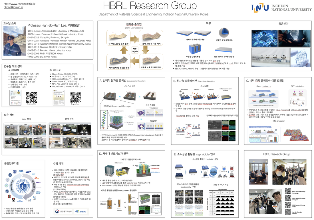
Research of HBRLRG
|
Professor Han-Bo-Ram Lee’s current research interests and topics are focused on understanding and controlling surface chemistry and reactions, and applying this knowledge to various applications of which properties could be improved by functionalization of surface from nanoscopic to macroscopic ranges.
Atomic-level theoretical calculations using density functional theory (DFT) and Monte Carlo (MC) simulation are employed, and experimental controls and functionalization of surface properties are realized by atomic layer deposition (ALD). Please find more details in the links as below |
|
atomic layer deposition
|
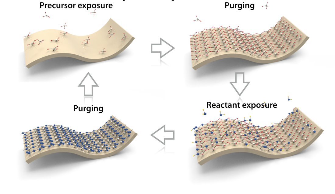
Atomic layer deposition (ALD) is a deposition technique employing surface self-saturation reaction during sequencial cycles.
One example of cyclic ALD reactions is depicted in the cartoon above. Due to the surface reactions of ALD, it has unique properties, such as excellent conformality and uniformity which are very important requirements for nanodevice fabrications. Therefore, ALD has been intensively studied for nanotechnology and nanoscience. For more information on ALD, please find review papers and online classes (Korean); |
|
- Review paper, Editorials, Virtual Issue
- “A Selective Toolbox for Nanofabrication,” Han-Bo-Ram Lee* and Stacey F. Bent, Chemistry of Materials, 2020, https://dx.doi.org/10.1021/acs.chemmater.0c00838
- “The Era of Atomic Crafting,” Han-Bo-Ram Lee*, Chemistry of Materials, 2019, http://doi.org/10.1021/acs.chemmater.9b00654
- "Atomic Layer Deposition on 2D Materials," Hyun Gu Kim and Han-Bo-Ram Lee*, Chemistry of Materials, 2017, http://dx.doi.org/10.1021/acs.chemmater.6b05103
- “Recent Advances in Atomic Layer Deposition,” Neil P. Dasgupta, Stacey Bent, Paul S. Weiss, and Han-Bo-Ram Lee*, Chemistry of Materials, 2017, http://dx.doi.org/10.1021/acs.chemmater.6b00673
- “Applications of Atomic Layer Deposition to Nanofabrication and Emerging Nanodevices,” Hyungjun Kim*, Han-Bo-Ram Lee, W.-J. Maeng, Thin Solid Films, 2009, https://doi.org/10.1016/j.tsf.2008.09.007
- Book Chapters
- “Back End of the Line,” in Atomic Layer Deposition for Semiconductors, Ed. Cheol Seong Hwang, Springer, ISBN:978-1-4614-8054-9, 10/19/2013 [DOI]
- “Chapter 9. Nanopatterning by Area-Selective Atomic Layer Deposition,” in Atomic Layer Deposition of Nanostructured Materials, Ed. Nicola Pinna and Mato Knez, Wiley-VCH (2011), ISBN: 978-3-527-32797-3, ½/2012 [DOI]
- Atomic Layer Deposition Short Course 2019 Spring in English
2. Introduction of ALD (https://youtu.be/F-A26ISXUOw)
3. Basic Growth Characteristics of ALD (https://youtu.be/pkVJ3o7E50U)
4. ALD Precursors & Reactants (https://youtu.be/-FIz_HVxsZI)
5. ALD Systems (https://youtu.be/bZ5jVkRUklI)
6. ALD Applications for Si Devices (https://youtu.be/KIj8uTzlrJw)
7. Atomic Crafting Beyond ALD (https://youtu.be/SjZAbPhlMoE)
- Atomic Layer Deposition Short Course 2019 Spring in Korean
2. Nucleation and Growth of Thin Films
3. Basics of ALD: Surface Reactions
4. Basics of ALD: Precursor & Reactant
5. Basics of ALD: ALD Equipments
6. ALP beyond ALD
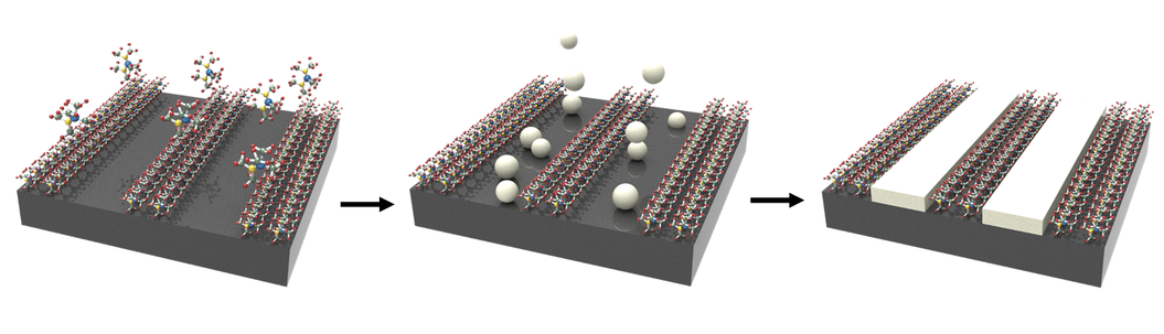
Area Selective deposition (ASD)
|
Research on area-selective atomic layer deposition (AS-ALD) has been intensively studied for nanotechnology and nanoscience in recent years. AS-ALD has been used as a simple patterning process with the several advantages of conventional ALD processes, such as uniformity, excellent conformality, and thickness control. In AS-ALD, surface properties are controlled to activate and deactivate ALD precursor adsorption, so that patterns along a same property domain are formed through selective deposition. For example, selective nucleation and growth occur on hydrophilic parts that have OH-terminated groups, which enhances chemical reaction with the precursors, so that the ALD reaction can be prevented by passivation of surface OH-terminated groups and termination with hydrophobic CH3 unreactive groups.
|
Presently, the HBRLG is trying to deposit a variety of precursor inhibitors on different substrates by ALD for area selective growth. For instance, the silicon oxide substrate coated with precursor inhibitors, yielding a hydrophobic and unreactive surface. AS-ALD of metals and metal oxides was found on part of the surface not covered with the hydrophobic and unreactive precursor inhibitors. Such type of AS-ALD may offers new opportunities for area selective growth in various nanofabrication schemes.
|
- For more information on AS-ALD, please find papers;
- “Effects of Al Precursors on Deposition Selectivity of Atomic Layer Deposition of Al2O3 using Ethanethiol Inhibitor” , Chemistry of Materials, online published, 9/28/2020, https://doi.org/10.1021/acs.chemmater.0c02798
- “A Selective Toolbox for Nanofabrication,” Han-Bo-Ram Lee* and Stacey F. Bent, Chemistry of Materials, 2020, https://dx.doi.org/10.1021/acs.chemmater.0c00838
- “The Era of Atomic Crafting,” Han-Bo-Ram Lee*, Chemistry of Materials, 2019, http://doi.org/10.1021/acs.chemmater.9b00654
- “Area-Selective Atomic Layer Deposition Using Si Precursors as Inhibitors,” Rizwan Khan, Bonggeun Shong, Byeong Guk Ko, Jae Kwang Lee, Hyunsoo Lee, Jeong Young Park, Il-Kwon Oh, Shimeles Shumi Raya, Hyun Min Hong, Kwun-Bum Chung, Erik J. Luber, Yoon-Seok Kim, Chul-Ho Lee, Woo-Hee Kim, and Han-Bo-Ram Lee*, Chemistry of Materials, 2018, http://doi.org/10.1021/acs.chemmater.8b02774
- Han-Bo-Ram Lee and Stacey F. Bent, “Chapter 9. Nanopatterning by Area-Selective Atomic Layer Deposition,” in Atomic Layer Deposition of Nanostructured Materials, Ed. Nicola Pinna and Mato Knez, Wiley-VCH (2011), ISBN: 978-3-527-32797-3, 1/2/2012, http://dx.doi.org/10.1002/9783527639915.ch9
- “High Quality Area-Selective Atomic Layer Deposition Co using Ammonia Gas as a Reactant,” Han-Bo-Ram Lee, Woo-Hee Kim, Jeong Won Lee, Kwang Heo, In Chan Hwang, Yongjun Park, Seunghun Hong, and Hyungjun Kim*, Journal of The Electrochemical Society, 157, D10-D15 (2010), 11/03/09, http://dx.doi.org/10.1149/1.3248002, [First author]
- “Degradation of Deposition Blocking Layer during Area Selective Plasma Enhanced Atomic Layer Deposition of Cobalt,” Han-Bo-Ram Lee, Woo-Hee Kim, Jeong Won Lee, Jaemin Kim, Inchan Hwang, and Hyungjun Kim*, Journal of Korean Physical Society, 56, 104-107 (2010), 12/01/09, http://dx.doi.org/10.3938/jkps.56.104, [First author]
- “Area Selective Atomic Layer Deposition by Microcontact Printing with a Water-Soluble Polymer,” Marja N. Mullings, Han-Bo-Ram Lee, Nathan Marchack, Xirong Jiang, Zhebo Chen, Yelena Gorlin, Kuang-Po Lin, and Stacey F. Bent*, Journal of The Electrochemical Society, 157, D600-D604 (2010), 10/04/10, http://dx.doi.org/10.1149/1.3491376, [Co-author]
- “Atomic Layer Deposition of Ni Thin Films and Application to Area-Selective Deposition,” Woo-Hee Kim, Han-Bo-Ram Lee, Kwang Heo, Young Kuk Lee, Taek-Mo Chung, Chang Gyoun Kim, Seunghun Hong, Jong Heo, and Hyungjun Kim*, Journal of The Electrochemical Society, 158, D1-D5 (2011), 11/09/10, http://dx.doi.org/10.1149/1.3504196, [Co-author]
- “Nucleation-controlled Growth of Nanoparticles by Atomic Layer Deposition,” Han-Bo-Ram Lee, Marja N. Mullings, Xirong Jiang, Bruce M. Clemens and Stacey F. Bent*, Chemistry of Materials, 24, 4051-4059 (2012), 10/19/2012, http://dx.doi.org/10.1021/cm3014978, [First author]
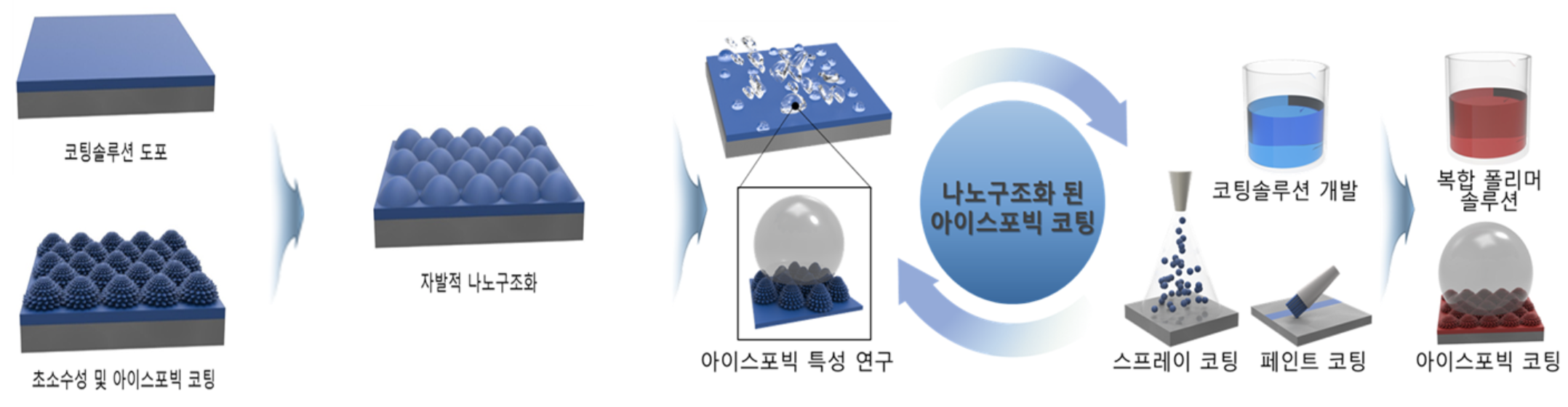
Superhydrophobicity & icepobicity
Surface hydrophobicity is a versatile surface property which can applied for many applications, such as water-repelling spray in car window, cooking frying pan, and water-proof coating. Most of hydrophobic coatings employ polymer coating materials due to their low fabrication cost and simple process scheme. However, the polymer coating has critical disadvantages, low thermal and mechanical stability, which are important requirements for industrial applications used in harsh environments.
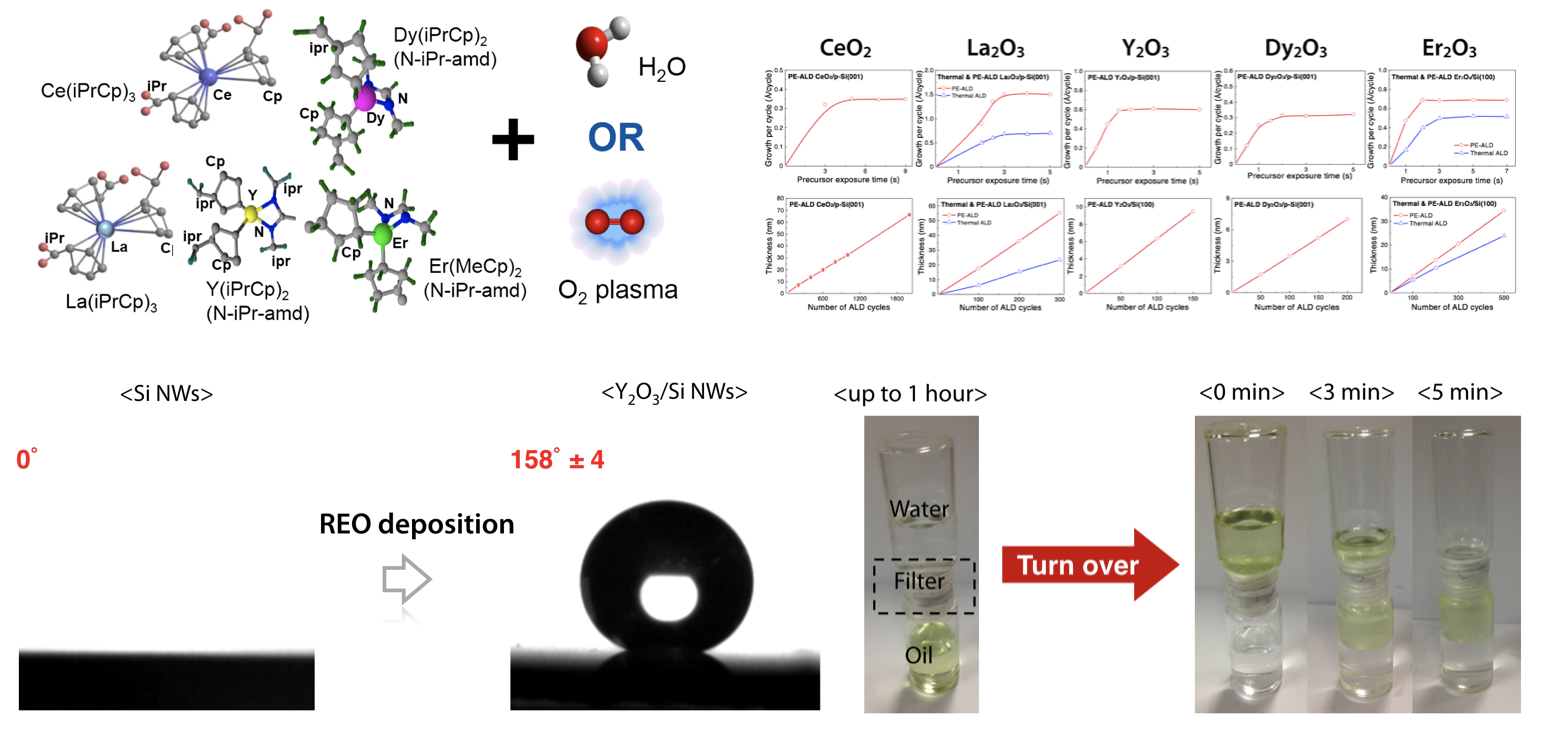
The HBRLRG is developing an inorganic hydrophobic material system using rare earth oxides (REOs). The REOs are synthesized by ALD as a thin film shape and applied to hydrophobic coating on various surfaces. Nanostructured Si surface, which has originally hydrophilic surface property, is readily changed into a superhydrophobic surface just by ALD REO coating. The surface energy of membrane filters is precisely tuned by controlling ALD REO thickness, and applied to oilwater separators. In addition, the ALD-REO-coated surface is utilized for liquid tweezer to selectively collect a specific liquid substance from the others.
Please find our previous results which are preliminary study for current research
- “Icephobic Coating through Self-formed Superhydrophobic Surface using Polymer and Microsize Particles,” \, ACS Applied Materials and Interfaces, online published, 1/4/2022, https://doi.org/10.1021/acsami.1c22404
- “Surface Energy Change of Atomic-scale Metal Oxide Thin Films by Phase Transformation,” Il-Kwon Oh, Li Zeng, Jae-Eun Kim, Jong-Seo Park, Kangsik Kim, Hyunsoo Lee, Seunggi Seo, Mohamed Rizwan Khan, Sangmo Kim, Chung Wung Park, Junghoon Lee, Bonggeun Shong, Zonghoon Lee, Stacey F. Bent, Hyungjun Kim, Jeong Young Park, and Han-Bo-Ram Lee*, ACS Nano, 2020, https://doi.org/10.1021/acsnano.9b07430
- “Preparation of a Hydrophobic Cerium Oxide Nanoparticle Coating via a Facile Solution Route,” Sumaira Yasmeen, Mohammad Rizwan Khan, Kiho Park, Yunshik Cho, Jang Wook Choi, Hyoung-Seok Moon, and Han-Bo-Ram Lee*, Ceramic International, 2020, https://doi.org/10.1016/j.ceramint.2020.01.268
- “Hydrophobicity of Rare Earth Oxides Grown by Atomic Layer Deposition,” Il-Kwon Oh, Kang-Sik Kim, Zonghoon Lee, Kyung-Yong Ko, Su Jeong Lee, Jae-Min Myung, Clement Lansalot-atras, Wontae Noh, Hyungjun Kim, and Han-Bo-Ram Lee, Chemistry of Materials, 2014, http://www.dx.doi.org/10.1021/cm503659d
- "Reversible Liquid Adhesion Switching of Superamphiphiphobic Pd-Decorated Ag Dendrites via Gas-induced Structural Changes", Dayeong Kim, Jungmok Seo, Sera shin, Soonil Lee, Kilsoo Lee, Hyeonjin Cho, Wooyoung Shim, Han-Bo-Ram Lee, and Taeyoon Lee, Chemistry of Materials, 6/30/2015, http://pubs.acs.org/doi/abs/10.1021/acs.chemmater.5b01038
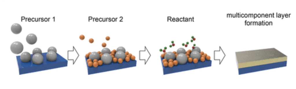
Atomic layer modulation
We proposed the concept of atomic layer modulation (ALM) based on precursor chemical reactivities and steric hindrance effects to fabricate multicomponent nanofilms. Because ALM employs consecutive precursor exposures followed by exposure to a counter reactant, the composition of ALM films is determined by the molecular size and chemical reactivities of the precursors.
- For more information on AS-ALD, please find papers;
2. “Growth Modulation of Atomic Layer Deposition HfO2 by Switching H2O and O3 Reactants Evaluation of Silicon Tetrahalide Precursors for Low-temperature Thermal Atomic Layer Deposition of Silicon Nitride,” Dalton Transactions, 11/23/2021, DOI: 10.1039/d1dt03465k
Emerging semiconductir device
Professor Han-Bo-Ram Lee

|
Han-Bo-Ram Lee, Ph.D
Professor Materials Science & Engineering, Incheon National University hbrlee[at]inu.ac.kr hbrlee[at]incheon.ac.kr Associate Editor Chemistry of Materials, ACS Publications (Link) lee-office[at]cm.acs.org Education
• Ph.D. in Materials Science and Engineering, POSTECH, Korea • B.S. in Materials Science and Engineering, Sungkyunkwan University, Korea Academic Appointment • Professor, Department of Materials Science and Engineering, Incheon National University, 3/2022 - current • Associate Professor, Department of Materials Science and Engineering, Incheon National University, 3/2017 - 2/2022 • Assistant Professor, Department of Materials Science and Engineering, Incheon National University, 2/2013 - 2/2017 |
Team
The HBRLRG is actively seeking for graduate students, postdocs, and undergraduate research assistants.
If you are interested in positions in HBRLRG, please submit your application (https://goo.gl/forms/3kYcLrsDL7ivoX4K2)
If you are interested in positions in HBRLRG, please submit your application (https://goo.gl/forms/3kYcLrsDL7ivoX4K2)

Arvind Patil Postdoctoral RESEARCHER patilarvindrao[at]gmail.com 
Zunair Masroor PHD STUDENT zunair[at]inu.ac.kr 
Min Gyu Lee MS STUDENT lee1123789[at]inu.ac.kr 
Min Kyeong Min UNDERGRAdUATE INTERN jddaimma[at]inu.ac.kr 
Kwang Yong An UNDERGRAdUATE INTERN anky0131[at]inu.ac.kr |

Summal Zoha PHD STUDENT summalzoha[at]inu.ac.kr 
Ngoc Le Trinh PHD STUDENT ngocletrinh[at]inu.ac.kr 
Da Bin Kong MS STUDENT rhdekqls1018[at]inu.ac.kr 
Won Joong Kim UNDERGRAdUATE INTERN kimwj1012[at]inu.ac.kr |

Bon Wook Gu PHD STUDENT Bonwookgu[at]inu.ac.kr 
Byung Chan Lee MS STUDENT leebc4345[at]inu.ac.kr 
Hye Won Park MS STUDENT dab7[at]inu.ac.kr 
Yoon Seo Choi UNDERGRADUATE INTERN light_045692[at]inu.ac.kr 
Hee Young Hwang ADMINISTRATION hhy20012001[at]gmail.com |
AlumNi
• Thang Chi Nguyen
- Ph.D. Course
- Department of Materials Science Engineering, INU, March 2018 ~ September 2023
• Julia Karnopp
- Ph.D. Course (Instituto Tecnológico de Aeronáutica)
- Research Student
- Department of Materials Science Engineering, INU, February 2023 ~ September 2023
• Mr. Min Sung Kim
- Undergraduate internship
- Department of Materials Science Engineering, INU, February 2020 ~ November 2022
• Ms. Sumaira Yasmeen
- Ph.D. Course
- Department of Materials Science Engineering, INU, September 2018 ~ October 2022
• Ms. Hyuna Bang
- Undergraduate internship
- Department of Materials Science Engineering, INU, December 2021 ~ March 2022
• Mr. Chan Hui Moon
- BS/MS Co-terminal Course
- Department of Materials Science Engineering, INU, March 2020 ~ February 2022
• Dr. Ansari Abu Saad
- Research professor
- Department of Materials Science Engineering INU, March 2021 ~November 2021
• Ms. Soo Hyun Choi
- Undergraduate student internship
- Department of Materials Science Engineering, INU, January 2021 ~ October 2021
• Ms. Dam Bin Oh
- Undergraduate student internship
- Department of Materials Science Engineering, INU, July 2020 ~ June 2021
• Ms. Min Hui Song
- Undergraduate student internship
- Department of Materials Science Engineering, INU, July 2020 ~ June 2021
• Dr. Mohammad Rizwan Khan
- Postdoctoral Fellow
- Department of Materials Science Engineering INU, March 2017 ~May 2021
• Mr. Geon Woo Park
- Undergraduate student internship
- Department of Materials Science Engineering, INU, Septmber 2020 ~ March 2021
• Mr. Hyeon Seok Oh
- Undergraduate student internship
- Department of Materials Science Engineering, INU, August 2020 ~ March 2021
• Mr. Joon Hyuk Ko
- Undergraduate student internship
- Department of Materials Science Engineering, INU, September 2020 ~ March 2021
• Ms. A Young Lim
- Undergraduate student internship
- Department of Materials Science Engineering, INU, February 2020 ~ March 2021
• Mr. Seok Jun Seo
- Undergraduate student internship
- Department of Materials Science Engineering INU, June 2020 ~March 2021
• Mr. Jin Sic Kim
- Undergraduate student internship
- Department of Materials Science Engineering INU, June 2020 ~March 2021
• Mr. Byeong Guk Ko
- MS Course
- Department of Materials Science Engineering INU, August 2017 ~February 2021
• Mr. Sang Hee Han
- MS Course
- Department of Materials Science Engineering INU, October 2019 ~August 2020
• Dr. Houda Gaiji
- Postdoctoral Fellow
- Department of Materials Science Engineering INU, July 2019 ~May 2020
• Mr. Jong Woo Shin
- MS Course
- Department of Materials Science Engineering INU, July 2018 ~May 2020
• Mr. Je Yung Ha
- Undergraduate student internship
- Department of Materials Science Engineering, INU, March 2019 ~February 2020
• Mr. Se Hyeon Song
- Undergraduate student internship
- Department of Materials Science Engineering, INU, March 2019 ~February 2020
• Dr. Jae Hong Yun
- Postdoctoral scholar
- Department of Materials Science Engineering, INU, March 2019 ~September 2019
• Mr. Jong Seo Park
- Ph.D. Course (Co-advising with Prof. Hyungjun Kim at Yonsei University)
- School of Electrical and Electronic Engineering, YU, September 2015 ~2019
• Mr. Hyun Gu Kim
- Ph.D. Course
- Department of Materials Science Engineering, INU, March 2014 ~August 2019
• Ms. Sun Hwa Kim
- Undergraduate student internship
- Department of Materials Science Engineering, INU, September 2015 ~ 2016
• Mr. Tae Hoon Park
- Undergraduate student internship
- Department of Materials Science Engineering, INU, September 2014 ~ 2015
• Ms. Min Ji Kim
- Undergraduate student internship
- Department of Materials Science Engineering, INU, September 2014 ~ 2015
• Mr. Song Min Gyu
- Undergraduate student internship
- Department of Materials Science Engineering, INU, September 2016 ~ 2017
• Mr. Tae Hee Han
- Undergraduate student internship
- Department of Materials Science Engineering, INU, September 2016 ~ 2017
•Mr. Young Hak Lee
- Undergraduate student internship
- Department of Materials Science Engineering, INU, January 2017 ~ 2018
•Mr. Yong Woon Lee
- Undergraduate student internship
- Department of Materials Science Engineering, INU, January 2017 ~ 2018
•Mr. Woo Hyeok Kwon
- Undergraduate student internship
- Department of Materials Science Engineering, INU, January 2017 ~ 2018
•Mr. Jae Kwang Lee
- Undergraduate student internship
- Department of Materials Science Engineering, INU, January 2017 ~ 2018
•Mr. Jae Hee Jeong
- Undergraduate student internship
- Department of Materials Science Engineering, INU, March 2018 ~ July 2018
•Mr. Tae Hwan Im
- Undergraduate student internship
- Department of Materials Science Engineering, INU, September 2017 ~ November 2018
•Ms. He Jin Lee
- Undergraduate student internship
- Department of Materials Science Engineering, INU, December 2017 ~ November 2018
•Mr. Seung Jae An
- Undergraduate student internship
- Department of Materials Science Engineering, INU, March 2018 ~ November 2018
- Ph.D. Course
- Department of Materials Science Engineering, INU, March 2018 ~ September 2023
• Julia Karnopp
- Ph.D. Course (Instituto Tecnológico de Aeronáutica)
- Research Student
- Department of Materials Science Engineering, INU, February 2023 ~ September 2023
• Mr. Min Sung Kim
- Undergraduate internship
- Department of Materials Science Engineering, INU, February 2020 ~ November 2022
• Ms. Sumaira Yasmeen
- Ph.D. Course
- Department of Materials Science Engineering, INU, September 2018 ~ October 2022
• Ms. Hyuna Bang
- Undergraduate internship
- Department of Materials Science Engineering, INU, December 2021 ~ March 2022
• Mr. Chan Hui Moon
- BS/MS Co-terminal Course
- Department of Materials Science Engineering, INU, March 2020 ~ February 2022
• Dr. Ansari Abu Saad
- Research professor
- Department of Materials Science Engineering INU, March 2021 ~November 2021
• Ms. Soo Hyun Choi
- Undergraduate student internship
- Department of Materials Science Engineering, INU, January 2021 ~ October 2021
• Ms. Dam Bin Oh
- Undergraduate student internship
- Department of Materials Science Engineering, INU, July 2020 ~ June 2021
• Ms. Min Hui Song
- Undergraduate student internship
- Department of Materials Science Engineering, INU, July 2020 ~ June 2021
• Dr. Mohammad Rizwan Khan
- Postdoctoral Fellow
- Department of Materials Science Engineering INU, March 2017 ~May 2021
• Mr. Geon Woo Park
- Undergraduate student internship
- Department of Materials Science Engineering, INU, Septmber 2020 ~ March 2021
• Mr. Hyeon Seok Oh
- Undergraduate student internship
- Department of Materials Science Engineering, INU, August 2020 ~ March 2021
• Mr. Joon Hyuk Ko
- Undergraduate student internship
- Department of Materials Science Engineering, INU, September 2020 ~ March 2021
• Ms. A Young Lim
- Undergraduate student internship
- Department of Materials Science Engineering, INU, February 2020 ~ March 2021
• Mr. Seok Jun Seo
- Undergraduate student internship
- Department of Materials Science Engineering INU, June 2020 ~March 2021
• Mr. Jin Sic Kim
- Undergraduate student internship
- Department of Materials Science Engineering INU, June 2020 ~March 2021
• Mr. Byeong Guk Ko
- MS Course
- Department of Materials Science Engineering INU, August 2017 ~February 2021
• Mr. Sang Hee Han
- MS Course
- Department of Materials Science Engineering INU, October 2019 ~August 2020
• Dr. Houda Gaiji
- Postdoctoral Fellow
- Department of Materials Science Engineering INU, July 2019 ~May 2020
• Mr. Jong Woo Shin
- MS Course
- Department of Materials Science Engineering INU, July 2018 ~May 2020
• Mr. Je Yung Ha
- Undergraduate student internship
- Department of Materials Science Engineering, INU, March 2019 ~February 2020
• Mr. Se Hyeon Song
- Undergraduate student internship
- Department of Materials Science Engineering, INU, March 2019 ~February 2020
• Dr. Jae Hong Yun
- Postdoctoral scholar
- Department of Materials Science Engineering, INU, March 2019 ~September 2019
• Mr. Jong Seo Park
- Ph.D. Course (Co-advising with Prof. Hyungjun Kim at Yonsei University)
- School of Electrical and Electronic Engineering, YU, September 2015 ~2019
• Mr. Hyun Gu Kim
- Ph.D. Course
- Department of Materials Science Engineering, INU, March 2014 ~August 2019
• Ms. Sun Hwa Kim
- Undergraduate student internship
- Department of Materials Science Engineering, INU, September 2015 ~ 2016
• Mr. Tae Hoon Park
- Undergraduate student internship
- Department of Materials Science Engineering, INU, September 2014 ~ 2015
• Ms. Min Ji Kim
- Undergraduate student internship
- Department of Materials Science Engineering, INU, September 2014 ~ 2015
• Mr. Song Min Gyu
- Undergraduate student internship
- Department of Materials Science Engineering, INU, September 2016 ~ 2017
• Mr. Tae Hee Han
- Undergraduate student internship
- Department of Materials Science Engineering, INU, September 2016 ~ 2017
•Mr. Young Hak Lee
- Undergraduate student internship
- Department of Materials Science Engineering, INU, January 2017 ~ 2018
•Mr. Yong Woon Lee
- Undergraduate student internship
- Department of Materials Science Engineering, INU, January 2017 ~ 2018
•Mr. Woo Hyeok Kwon
- Undergraduate student internship
- Department of Materials Science Engineering, INU, January 2017 ~ 2018
•Mr. Jae Kwang Lee
- Undergraduate student internship
- Department of Materials Science Engineering, INU, January 2017 ~ 2018
•Mr. Jae Hee Jeong
- Undergraduate student internship
- Department of Materials Science Engineering, INU, March 2018 ~ July 2018
•Mr. Tae Hwan Im
- Undergraduate student internship
- Department of Materials Science Engineering, INU, September 2017 ~ November 2018
•Ms. He Jin Lee
- Undergraduate student internship
- Department of Materials Science Engineering, INU, December 2017 ~ November 2018
•Mr. Seung Jae An
- Undergraduate student internship
- Department of Materials Science Engineering, INU, March 2018 ~ November 2018
Papers
|
|
: Total number of papers
: h index
:Total number of citations
|
2024
121. “Si precursor inhibitors for area selective deposition of Ru," Bonwook Gu, Sumaira Yasmeen, Geun-Ha Oh, Il-Kwon, Youngho Kang, Han-Bo-Ram Lee*, Applied Surface Science,10/1/2024, https://doi.org/10.1016/j.apsusc.2024.160530, [Corresponding author]
120. “Organothiol Inhibitor Instigated Passivation of Multiple Substrates for Area-Selective Atomic LayerDeposition of HfO2,” Summal Zoha, Fabian Pieck, Bonwook Gu, Ralf Tonner-Zech*, and Han-Bo-Ram Lee*, Chemistry of Materials, 2/22/2024, https://pubs.acs.org/doi/10.1021/acs.chemmater.3c02525, [Corresponding author]
119. “Facile Approach for Designing Icephobic Coatings using Polymers/Silica Nanoparticle Composites via Self-Formation of Superhydrophobic Surfaces,” Aravind H. Patil, Ngoc Le Trinh, Hackwon Do,Houda Gaiji,Youngho Kang, Joohan Lee, Changhyun Chung*, and Han-Bo-Ram Lee*, Advanced Materials Interfaces, 2/7/2024, https://doi.org/10.1002/admi.202300919, [Corresponding author]
2023
118. “Area Selective Deposition of Ruthenium Using Homometallic Precursor Inhibitor,” Chi Thang Nguyen, EunHyoung Cho, Ngoc Le Trinh, Bonwook Gu, Mingyu Lee, Sunghee Lee, Jeong Yub Lee, Youngho Kang, and Han-Bo-Ram-Lee*, Chemistry of Materials, online published, 7/3/2023, https://doi.org/10.1021/ acs.chemmater.3c00525, [Corresponding author]
117. "Borderless Collaboration in Materials Chemistry for an Industrial Ecosystem in the Semiconductor Industry," Han-Bo-Ram Lee* and Seiyon Kim, Chemistry of Materials, 6/13/2023, https://doi.org/10.1021/acs.chemmater.3c01077, [Corresponding author]
116. “Self-formation of a Ru/ZnO Multifunctional Bilayer through Area-Selective Atomic Layer Deposition for Interconnect Technology,” Yuki Mori, Taehoon Cheon, Yohei Kotsugi, Youn-Hye Kim, Yejin Park, Mohd Zahid Ansari, Debananda Mohapatra, Yujin Jang, Jong-Seong Bae, Woobin Kwon, Gahui Kim, Young-Bae Park, Han-Bo-Ram Lee, Wooseok Song,* and Soo-Hyun Kim*, Small, 2300290 (2023), 5/1/2023, https://doi.org/ 10.1002/smll.202300290, [Co-author]
115. "Dysprosium Incorporation for Phase Stabilization of Atomic-Layer-Deposited HfO2 Thin Films,” Yujin Lee, Kangsik Kim, Zonghoon Lee, Hong-Sub Lee, Han-Bo-Ram Lee, Woo-Hee Kim*, Il-Kwon Oh*, and Hyungjun Kim*, Chemistry of Materials, published online, 3/16/2023, https://doi.org/10.1021/ acs.chemmater.2c02862, [Co-author]
2022
114. “Gradient Area-Selective Deposition for Seamless Gap-filling in 3D Nanostructures through Surface Chemical Reactivity Control,” Chi Thang Nguyen, Eun-Hyoung Cho, Bonwook Gu, Sunghee Lee, Hae-Sung Kim, Jeongwoo Park, Neung-Kyung Yu, Sangwoo Shin, Bonggeun Shong, Jeong Yub Lee, and Han-BoRam-Lee*, Nature Communications, 13, 9579 (2022), 12/9/2022, https://doi.org/10.1038/ s41467-022-35428-6, [Corresponding author]
113. “Atomic Layer Deposition Beyond Thin Film Deposition Technology,” Sumaira Yasmeen, Seung Wook Ryu, Sung-Hoon Lee, and Han-Bo-Ram-Lee*, 2200876 (2022), 10/10/2022, Advanced Materials Technologies, https://doi.org/10.1002/ admt.202200876, [Corresponding author]
112. "Journal of the American Chemical Society, 2022, “Elucidating Reaction Mechanism of Atomic Layer Deposition of Al2O3 with a Series of Al(CH)xCl3-x and Al(CyH2y+1)3 Precursors,” Bonwook Gu, Ngoc Le Trinh, Chi Thang Nguyen, Sumaira Yasmeen, Houda Gaiji, Youngho Kang, and Han-Bo-Ram Lee*, Chemistry of Materials, 8/26/2022, https://doi.org/10.1021/ jacs.2c03752, [Corresponding author]
111. “Icephobic Coating through Self-formed Superhydrophobic Surface using Polymer and Microsize Particles,” Chan Hui Moon, Sumaira Yasmeen, Kiho Park, Gaiji Houda, Changhyun Chung, Hyoungkwon Kim, Hyoung-Seok Moon, Jang Wook Choi, and Han-Bo-Ram-Lee*, ACS Applied Materials and Interfaces, online published, 1/4/2022, https://doi.org/10.1021/acsami.1c22404, [Corresponding author]
2021
110. “Growth Modulation of Atomic Layer Deposition HfO2 by Switching H2O and O3 Reactants Evaluation of Silicon Tetrahalide Precursors for Low-temperature Thermal Atomic Layer Deposition of Silicon Nitride,” Byeong Guk Ko, Chi Thang Nguyen, Bonwook Gu, Mohammad Rizwan Khan, Kunwoo Park, Jungwon Park, Bonggeun Shong, Han-Bo-Ram Lee*, Dalton Transactions, 11/23/2021, DOI: 10.1039/d1dt03465k, [Corresponding author]
109. “Evaluation of Silicon Tetrahalide Precursors for Low-temperature Thermal Atomic Layer Deposition of Silicon Nitride,” Neung-Kyung Yu, Chan Hui Moon, Jeongwoo Park, Han-Bo-Ram Lee*, and Bonggeun Shong*, Applied Surface Science, online published, 7/12/2021, https://doi.org/10.1016/j.apsusc.2021.150603 [Corresponding author]
108. “Toward Enhanced Humidity Stability of Triboelectric Mechanical Sensors via Atomic Layer Deposition,” Wook Kim, Sumaira Yasmeen, Nguyen Chi Thang, Han-Bo-Ram Lee*, Dukhyun Choi*, Nanomaterials, 11(7), 1795, 7/9/2021, https://doi.org/10.3390/nano11071795, [Corresponding author]
107. “Atomic Layer Modulation of Multicomponent Thin Films through Combination of Experimental and Theoretical Approaches,” Chi Thang Nguyen, Bonwook Gu, Taehoon Cheon, Jeongwoo Park, Mohammad Rizwan Khan, Soo-Hyun Kim, Bonggeun Shong, and Han-Bo-Ram Lee*, Chemistry of Materials, online published, 06/10/2021, https://doi.org/10.1021/acs.chemmater.1c00508, [Corresponding author]
2020
106. “Effects of Al Precursors on Deposition Selectivity of Atomic Layer Deposition of Al2O3 using Ethanethiol Inhibitor,” Hyun Gu Kim, Miso Kim, Bonwook Gu, Mohammad Rizwan Khan, Byeong Guk Ko, Sumaira Yasmeen, Chang Su Kim, Se-Hun Kwon, Jiyong Kim, Junhyuck Kwon, Kwangseon Jin, Byungchul Cho, J. -S. Chun, Bonggeun Shong*, and Han-Bo-Ram Lee*, Chemistry of Materials, online published, 9/28/2020, https://doi.org/10.1021/acs.chemmater.0c02798, [Corresponding author]
105. “Promoting Lithium Electrodeposition Towards the Bottom of 3-D Copper Meshes in Lithium-based Batteries,” Sujung Kim, Yena Kim, Taegyu Jang, Chi Thang Nguyen, Han-Bo-Ram Lee, and Hye Ryung Byon*, Journal of Power Source, online published, 7/8/2020, https://doi.org/10.1016/ j.jpowsour.2020.228495 [Co-author]
104. “Atomic Level Deposition to Extend Moore’s Law and Beyond,” Rong Chen*, Yi-Cheng Li, Jia-Ming Cai, Kun Cao, and Han-Bo-Ram Lee, International Journal of Extreme Manufacturing, 2 (2), 022002-1 (2020), 4/30/2020, https://doi.org/10.1088/2631-7990/ab83e0, [Co-author]
103. "A Selective Toolbox for Nanofabrication", Han-Bo-Ram Lee* and Stacey F. Bent, Chemistry of Materials, https://doi.org/10.1021/acs.chemmater.0c00838, [Corresponding author]
102. “Ultrathin Effective TiN Protective Films Prepared by Plasma-enhanced Atomic Layer Deposition for High Performance Metallic Bipolar Plates of Polymer Electrolyte Membrane Fuel Cells,” Woo-Jae Lee, Eun-Young Yun, Han-Bo-Ram Lee, Suck Won Hong*, and Se-Hun Kwon*, Applied Surface Science, 519, 146215 (2020), 3/27/2020, https://doi.org/10.1016/j.apsusc.2020.146215, [Co-author]
101. "Tunable Color Coating of E-Textiles by Atomic Layer Deposition of Multilayer TiO2/Al2O3 Films", Mohammad Rizwan Khan, Hyun Gu Kim, Jong Seo Park, Jong Woo Shin, Chi Thang Nguyen and Han-Bo-Ram Lee*, Languir (2020), https://dx.doi.org/10.1021/acs.langmuir.9b03988, [Corresponding author]
100. "Preparation of a hydrophobic cerium oxide nanoparticle coating with polymer binder via a facile solution route", Sumaira Yasmeen, Mohammad Rizwan Khan, Kiho Park, Yunshik Cho, Jang Wook Choi, Hyoung-Seok Moon and Han-Bo-Ram Lee*, Ceramics International, [Corresponding author]
99. “Surface Energy Change of Atomic-scale Metal Oxide Thin Films by Phase Transformation,” Il-Kwon Oh, Li Zeng, Jae-Eun Kim, Jong-Seo Park, Kangsik Kim, Hyunsoo Lee, Seunggi Seo, Mohammad Rizwan Khan, Sangmo Kim, Chung Wung Park, Junghoon Lee, Bonggeun Shong, Zonghoon Lee, Stacey F. Bent, Hyungjun Kim, Jeong Young Park and Han-Bo-Ram Lee*, ACS Nano, 2020, https://doi.org/10.1021/acsnano.9b07430, [Corresponding author]
98. “Effect of Molecular Backbone Structure on Gas Phase Coupling Chemistry of (Thio)urea/urethane,” Shimeles Shumi Raya, Abu Saad Ansari, Sung Gu Kang, Han-Bo-Ram Lee* and Bonggeun Shong*, Organic Coating, 140, 105509 (2020), https://doi.org/10.1016/j.porgcoat.2019.105509, [Corresponding author]
2019
97. “Reaction Mechanism of Pt Atomic Layer Deposition on Various Textile Surfaces,” Il-Kwon Oh, Jong Seo park, Rizwan Khan, Kangsik Kim, Zonghoon Lee, Bonggeun Shong and Han-Bo-Ram Lee*, Chemistry of Materials, 10/23/2019, http://doi.org/10.1021/acs.chemmater.9b03171 [Corresponding author]
96. “Science against Pseudoscience,” Han-Bo-Ram Lee*, Chemistry of Materials, 31 (18), 7113-7115 (2019), 9/24/2019, https://doi.org/10.1021/acs.chemmater.9b03134, [Corresponding author]
95. “Moisture Barrier Properties of Low-Temperature Atomic Layer Deposited Al2O3 using Various Oxidants,” Taewook Nam, Haksoo Lee, Seunggi Seo, Sung Min Cho, Bonggeun Shong, Han-Bo-Ram Lee, Hyungjun Kim*,Ceramics International, published online, 6/20/2019, https://doi.org/10.1016/j.ceramint.2019.06.156 [Coauthor]
94. “Thermal Atomic Layer Deposition of Metallic Ru using H2O as a Reactant,” Thang Chi Nguyen, Jaehong Yoon, Rizwan Khan, Bonggeun Shong* and Han-Bo-Ram Lee*, Applied Surface Science, published online, 5/21/2019, https://doi.org/10.1016/j.apsusc.2019.05.242 [Corresponding author]
93. “Analysis of Defect Recovery in Reduced Graphene Oxide and Its Application as a Heater for Self-Healing Polymers,” Hyun Gu Kim, Il-Kwon Oh, Seungmin Lee, Sera Jeon, Hyunyong Choi, Kwanpyo Kim, Joo Ho Yang, Jae Woo Chung, Jaekwang Lee, Woo-Hee, Kim*, and Han-Bo-Ram Lee*, in revision, ACS Applied Materials and Interfaces, published online, 4/9/2019, http://doi.org/10.1021/acsami.8b19955 [Corresponding author]
92. “The Era of Atomic Crafting,” Han-Bo-Ram Lee*, Chemistry of Materials, 31 (5), 1471-1472 (2019), 3/12/2019, http://doi.org/10.1021/acs.chemmater.9b00654 [Corresponding author]
2018
91. “Area-Selective Atomic Layer Deposition Using Si Precursors as Inhibitors,” Rizwan Khan, Bonggeun Shong, Byeong Guk Ko, Jae Kwang Lee, Hyunsoo Lee, Jeong Young Park, Il-Kwon Oh, Shimeles Shumi Raya, Hyun Min Hong, Kwun-Bum Chung, Erik J. Luber, Yoon-Seok Kim, Chul-Ho Lee, Woo-Hee Kim, and Han-Bo-Ram Lee*, Chemistry of Materials, 30 (21), 7603-7610 (2018), 10/11/2018, http://doi.org/ 10.1021/acs.chemmater.8b02774, [Corresponding author]
90. “Area-Selective Atomic Layer Deposition Using Si Precursors as Inhibitors,” Rizwan Khan, Bonggeun Shong, Byeong Guk Ko, Jae Kwang Lee, Hyunsoo Lee, Jeong Young Park, Il-Kwon Oh, Shimeles Shumi Raya, Hyun Min Hong, Kwun-Bum Chung, Erik J. Luber, Yoon-Seok Kim, Chul-Ho Lee, Woo-Hee Kim, and Han-Bo-Ram Lee*, Chemistry of Materials, 30 (21), 7603-7610 (2018), 10/11/2018, http://doi.org/10.1021/acs.chemmater.8b02774, [Corresponding author]
89. “Analysis of Defect Recovery in Reduced Graphene Oxide and Its Application as a Heater for Self-Healing Polymers,” Hyun Gu Kim, Il-Kwon Oh, Seungmin Lee, Sera Jeon, Hyunyong Choi, Kwanpyo Kim, Joo Ho Yang, Jae Woo Chung, Jaekwang Lee, Woo-Hee, Kim*, and Han-Bo-Ram Lee*, in revision, ACS Applied Materials and Interfaces, [Corresponding author]
88. “Amorphous TiO2/p-Si Heterojunction Photodiode prepared by Low-temperature Atomic Layer Deposition,” Jaehong Yoon, Rizwan Khan, Il-Kwon Oh, Hyungjun Kim*, and Han-Bo-Ram Lee*, Nanoscience and Nanotechnology Letters, 10(5-6), 779-783 (2018), 5/1/2018, https://doi.org/10.1166/nnl.2018.2638, [Corresponding author]
87. “Surface Wettability of Nitrogen-doped TiO2 Films by Atomic Layer Deposition using NH4OH as a Doping Source,” Rizwan Khan, Kyung Yong Ko, Jong Seo Park, Hyungjun Kim*, and Han-Bo-Ram Lee*, Nanoscience and Nanotechnology Letters, 10(5-6), 779-783 (2018), 5/1/2018, https://doi.org/10.1166/nnl.2018.2663, [Corresponding author]
86. “Comparative Study of the Growth Characteristics and Electrical Properties of Atomic-Layer-Deposited HfO2 Films obtained from Metal Halide and Amide Precursors,” Il-Kwon Oh, Bo-Eun Park, Seunggi Seo, Byung Chul Yeo, Jukka Tanskanen, Han-Bo-Ram Lee, Woo-Hee Kim, and Hyungjun Kim*, published online, 6/29/2018, Journal of Materials Chemistry C, https://doi.org/10.1039/C8TC01476K, [Co-author]
85. “Effect of h-BN Coating on Nucleate Boiling Heat Transfer Performance in Pool Boiling,” Ji Min Kim, ByeongTak Kong, Somchai Wongwises, Han-Bo-Ram Lee, and Ho Seon Ahn*, Experimental Thermal and Fluid Science, 93, 12-19 (2018), 5/14/2018, https://doi.org/10.1016/j.expthermflusci.2018.05.010, [Coauthor]
84. “Circular Double-Patterning Lithography using a Block Copolymer Template and Atomic Layer Deposition,” Zhixin Wan, Ha Jin Lee, Hyun Gu Kim, Gyeong Cheon Jo, Woon Ik Park, Seung Wook Ryu, Han-Bo-Ram Lee*, and Se-Hun Kwon*, published online, Advanced Materials Interfaces, 4/20/2018, https://doi.org/10.1002/admi. 201800054, [Corresponding author]
83. “Interlayer-assisted Atomic Layer Deposition of MgO as a Magnetic Tunneling Junction Insulators,” Seung Wook Ryu, Jeong-Gyu Song, Hyun Gu Kim, Hyungjun Kim*, and Han-Bo-Ram Lee*, online published, 3/7/2018, https://doi.org/10.1016/j.jallcom.2018.03.021, Journal of Alloys and Compound, [Corresponding author]
82. “Amorphous TiO2/p-Si Heterojunction Photodiode prepared by Low-temperature Atomic Layer Deposition,” Jaehong Yoon, Rizwan Khan, Il-Kwon Oh, Hyungjun Kim*, and Han-Bo-Ram Lee*, accepted to Nanoscience and Nanotechnology Letters, [Corresponding author]
81. “Copper Indium Selenide Water Splitting Photoanodes with Artificially Designed Heterophasic Blended Structure and Their High Photoelectrochemical Performances,” Joo Sung Kim, Seung Ki Baek, Young Been Kim, Hyun Woo Do, Yong Hun Kwon, Sung Woon Cho, Young Dae Yun, Jae Hong Yoon, Han-Bo-Ram Lee, Sang-Woo Kim, and Hyung Koun Cho*, Nano Energy, published online, 1/18/2018, http://dx.doi.org/10.1021/acs.chemmater.7b04371 [Co-author]
80. "Water-Erasable Memory Device for Security Applications Prepared by the Atomic Layer Deposition of GeO2" Chang Mo Yoon, Il Kwon Oh, Yu jin Lee, Jeong Gyu Song, Su Jeong Lee, Jae Min Myoung, Hyun Gu Kim, Hyoung Seok Moon, Bong Geun Shong, Han Bo Ram Lee and Hyung jun Kim , Journal of Chemistry of Materials, published online, January 12, 2018, https://doi.org/10.1016/j.nanoen.2018.01.023
2017
79. "Effect of porous graphene networks and micropillar arrays on boiling heat transfer performance" Ji Min Kim, Su Cheong Park, ByeongTak Kong, Han-Bo-Ram Lee, Ho Seon Ahn, journal of Experimental Thermal and Fluid Science, https://doi.org/10.1016/j.expthermflusci.2017.12.029
78. "Cobalt titanium nitride amorphous metal alloys by atomic layer deposition", Tae wook Nam, Chang wan Lee, Taehoon Cheon, Woo Jae Lee, Soo-Hyun Kim, Se-Hun Kwon, Han-Bo-Ram Lee, Hyungjun Kim, Journal of Alloys and Compounds, 15 march 2018 pp. 684-692, DOI: http://doi.org/10.1016/j.jallcom.2017.12.023
77. " Dual Role of Sb-Incorporated Buffer Layers for High Efficiency Cuprous Oxide Photocathodic Performance: Remarkably Enhanced Crystallinity and Effective Hole Transport", Seung Ki Baek, Joo Sung Kim, Young Been Kim, Jae Hong Yoon, Han-Bo-Ram Lee , and Hyung Koun Cho , ACS Sustainable Chem. Eng., 2017, 5 (9), doi: http://pubs.acs.org/doi/abs/10.1021/acssuschemeng.7b01889
76. " Reaction Mechanism of Area-Selective Atomic Layer Deposition for Al2O3 Nanopatterns", Seunggi Seo, Byung Chul Yeo, Sang Soo Han , Chang Mo Yoon, Joon Young Yang, Jonggeun Yoon§, Choongkeun Yoo§, Ho-jin Kim§, Yong-baek Lee§, Su Jeong Lee∥, Jae-Min Myoung∥ , Han-Bo-Ram Lee, Woo-Hee Kim, Il-Kwon Oh*†, and Hyungjun Kim* , ACS Appl. Mater. Interfaces, Article ASAP, November 7, (2017), DOI: http://pubs.acs.org/doi/abs/10.1021/acsami.7b13365
75. " Conduction mechanism change with transport oxide layer thickness in oxide hetero-interface diode", Bu-il Nam, Jong Seo Park, Keon-Hee Lim, Yong-keon Ahn, Jinwon Lee, Jun-woo Park, Nam-Kwang Cho, Donggun Lee, Han-Bo-Ram Lee, and Youn Sang Kim, App. Phys. Lett, (2017), doi: http://dx.doi.org/10.1063/1.4996862
74. " Atomic layer deposition of Y-stabilized ZrO2 for advanced DRAM capacitors," Bo-Eun Park, Il-Kwon Oh, Chandreswar Mahata, ChangWan Lee, David Thompson,
Han-Bo-Ram Lee, Wan Joo Maeng, Hyungjun Kim, Journal of Alloys and Compounds, (2017) , Doi : 10.1016/j.jallcom.2017.06.036
73. "Atomic Layer Deposition on 2D Materials," Hyun Gu Kim and Han-Bo-Ram Lee*, Chemistry of Materials,(2017), http://dx.doi.org/10.1021/acs.chemmater.6b05103, [Corresponding author]
72. "Nanoconfined Atomic Layer Deposition of TiO2/Pt Nanotubes: Toward Ultrasmall Highly Efficient Catalytic Nanorockets,” Jinxing Li, Wenjuan Liu, Jiyuan Wang, Isaac Rozen, Sha He, Chuanrui Chen, Hyun Gu Kim, Ha-Jin Lee, Han-Bo-Ram Lee, Se-Hun Kwon, Tianlong Li, Longqiu Li*, Yongfeng Mei*, and Joseph Wang*, Advanced Functional Materials, 1700598 (2017), http://dx.doi.org/10.1002/adfm.201700598, [Co-author]
71. “A Composite Layer of Atomic-Layer-Deposited Al2O3 and Graphene for Flexible Moisture Barrier,” Taewook Nam, You
ngju Park, Seung-Woo Seo, Il-Kwon Oh, Jong-Hyun Ahn, Sung Min Cho, Hyungjun Kim*, and Han-Bo-Ram Lee*, Carbon, 116, 553-561 (2017), 2/17/2017, http://dx.doi.org/10.1016/j.carbon.2017.02.023, [Corresponding author]
70. “Atomic Layer Deposition of 1D and 2D Nickel Nanostructures on Graphite,” Seung Wook Ryu† & Jaehong Yoon† & Hyoung-Seok Moon†, Bonggeun Shong, Hyungjun Kim, and Han-Bo-Ram Lee*, Nanotechnology, 28(11), 115301 (2017), 2/13/2017, https://doi.org/10.1088/1361-6528/aa5aec, †Equal contribution, [Corresponding author]
69. “Distribution of Oxygen Functional Groups of Graphene Oxide obtained from Low-temperature Atomic Layer Deposition of Titanium Oxide,” Dong Seok Shin†, Hyun Gu Kim†, Ho Seon Ahn†, Hu Young Jeong, Yeon Jung Kim, Dorj Odkhuu, Han-Bo-Ram Lee* and Byung Hoon Kim*, RSC Advances, 7, 13979-13984 (2017), 3/2/2017, http://dx.doi.org/10.1039/C7RA00114B, [Corresponding author]
68. “Vapor Phase Synthesis of TaS2 Nanocrystals with Iodine as Transport Agent,” Gangtae Jin, Chaeeun Kim, Hyunjin Jo, Se-Hun Kwon, Seong-Jun Jeong, Han-Bo-Ram Lee*, and Ji-Hoon Ahn*, Japanese Journal of Applied Physics, 56, 045501 (2017), 3/3/2017, https://doi.org/10.7567/JJAP.56.045501, [Corresponding author]
2016
67. “Self-Limiting Layer Synthesis of Transition Metal Dichalcogenides,” Youngjun Kim, Jeong-Gyu Song, Yong Ju Park, Gyeong Hee Ryu, Su Jeong Lee, Jin Sung Kim, Pyo Jin Jeon, Chang Wan Lee, Whang Je Woo, Taejin Choi, Hanearl Jung, Han-Bo-Ram Lee, Jae-Min Myoung, Seongil Im, Zonghoon Lee, Jong-Hyun Ahn, Jusang Park, and Hyungjun Kim*, Scientific Reports, 6, 18754, 1/4/2016, http://dx.doi.org/10.1038/srep18754, [Co-author]
66. “Complementary Unipolar WS2 Field Effect Transistors using Fermi Level De-pinning Layers,” Woojin Park, Yonghun Kim, Ukjin Jung, Jin Ho Yang, Chunhum Cho, Yun Ji Kim, Syed Mohammad Najib Hasan, Hyun Gu Kim, Han-Bo-Ram Lee, and Byoung Hun Lee*, Advanced Electronic Materials, 2(2), 1-5 (2016), 2/12/2016, http://dx.doi.org/10.1002/aelm.201500278, [Co-author]
65. “Growth Characteristics and Electrical Properties of SiO2 Thin Films Prepared using Plasma-Enhanced Atomic Layer Deposition and Chemical Vapor Deposition with an Aminosilane Precursor,” Hanearl Jung, Woo-Hee Kim, Il-Kwon Oh, Chang-Wan Lee, Clement Lansalot-Matras, Su Jeong Lee, Jae-Min Myoung, Han-Bo-Ram Lee, and Hyungjun Kim*, Journal of Materials Science, 51(11), 5082-5091 (2016), 2/22/2016, http://dx.doi.org/10.1007/s10853-016-9811-0, [Co-author]
64. “Wafer-scale, Conformal and Direct Growth of MoS2 Thin Films by Atomic Layer Deposition,” Yujin Jang, Seungmin Yeo, Han-Bo-Ram Lee, Hyungjun Kim, and Soo-Hyun Kim*, Applied Surface Science, 365, 160-165 (2016), 3/1/2016, http://dx.doi.org/10.1016/j.apsusc.2016.01.038, [Co-author]
63. “Plasma Enhanced Atomic Layer Deposition of SnO2 Thin Films using SnCl4 Precursor and Oxygen Plasma,” Dong Kwon Lee, Zhixin Wan, Jong-Seong Bae, Han-Bo-Ram Lee, Ji-Hoon Ahn, Sang-Deok Kim, Jayong Kim, and Se-Hun Kwon*, Materials Letters, 166, 163-166 (2016), 3/1/2016, http://dx.doi.org/doi:10.1016/j.matlet.2015.12.049, [Co-author]
62. “Effects of Cl-based Ligand Structures on Atomic Layer Deposited HfO2,” Bo-Eun Park, Il-Kwon Oh, Chang Wan Lee, Gyeongho Lee, Young-Han Shin, Clement Lansalot-Matras, Wontae Noh, Hyungjun Kim*, and Han-Bo-Ram Lee*, Journal of Physical Chemistry C, 120(11), 5958–5967 (2016), 3/11/2016, http://dx.doi.org/10.1021/acs.jpcc.5b05286, [Corresponding author]
61. “Effects of Diffusion Barrier on Cu-gate ZnO:N Thin Film Transistors,” Whang Je Woo, Taewook Nam, Hanearl Jung, Il-Kwon Oh, Han-Bo-Ram Lee, Wanjoo Maeng, and Hyungjun Kim*, IEEE Electron Device Letters, 37(5), 599-602 (2016), 3/31/2016, http://dx.doi.org/10.1109/LED.2016.2549035, [Co-author]
60. ”A Controlled Growth of WNx and WCx Films Prepared by Atomic Layer Deposition,” Jun Beom Kim, Byeong Hyeon Jang, Hyun-Jung Lee, Won Seok Han, Do-Joong Lee, Han-Bo-Ram Lee, Tae Eun Hong, and Soo-Hyun Kim*, Materials Letters, 168, 218-222 (2016), 4/1/2016, http://dx.doi.org/10.1016/j.matlet.2016.01.071, [Co-author]
59. “Comparison of Hydrogen Sulfide Gas and Sulfur Powder for Synthesis of Molybdenum Disulfide Nanosheets,” Jusang Park, Jeonggyu Song, Taejin Choi, Sangwan Sim, Hyunyong Choi, Sang Wook Han, Han-Bo-Ram Lee, Soo-Hyun Kim, and Hyungjun Kim*, Current Applied Physics, http://dx.doi.org/10.1016/j.cap.2016.03.022, 16(7), 691-695 (2016), 4/1/2016, [Co-author]
58. “Highly-conformal Nanocrystalline Molybdenum Nitride Thin Films by Atomic Layer Deposition using a Newly Synthesized Precursor as a Diffusion Barrier against Cu,” Yujin Jang, Jun Beom Kim, Tae Eun Hong, So Jeong Yeo, Sunju Lee, Eun Ae Jung, Bo Keun Park, Taek-Mo Chung, Chang Kim, Do-Joong Lee, Han-Bo-Ram Lee, and Soo-Hyun Kim*, Journal of Alloys and Compounds, 663, 651-658 (2016), 4/5/2016, http://dx.doi.org/10.1016/j.jallcom.2015.12.148, [Co-author]
57. “Formation of Ni Silicide from Atomic Layer Deposited Ni,” Jaehong Yoon, Soo Hyeon Kim, Hangil Kim, Soohyun Kim, Hyungjun Kim*, and Han-Bo-Ram Lee*, Current Applied Physics, 16(7), 720-725 (2016), 4/6/2016, http://dx.doi.org/10.1016/j.cap.2016.04.005, [Corresponding author]
56. “Recent Advances in Atomic Layer Deposition,” Neil P. Dasgupta, Stacey Bent, Paul S. Weiss, and Han-Bo-Ram Lee*, Chemistry of Materials, 28(7), 1943–1947 (2016), 4/12/2016, http://dx.doi.org/10.1021/acs.chemmater.6b00673, [Corresponding author]
55. “A Facile Method for Selective Healing of Graphene Defects Based on a Galvanic Displacement Reaction,” Juree Hong, Jae-Bok Lee, Sanggeun Lee, Jungmok Seo, Hyunsoo Lee, Jeong Young Park, Tae-il Seo, Jong-Hyun Ahn, Taeyoon Lee*, and Han-Bo-Ram Lee*, NPG Asia Materials, 8, e262 (2016), 4/15/2016, http://dx.doi.org/10.1038/am.2016.42, [Corresponding author]
54. “High Efficiency n-Si/p-Cu2O Core–shell Nanowires Photodiode Prepared by Atomic Layer Deposition of Cu2O on Well-ordered Si Nanowires Array,” Hangil Kim, Soo-Hyun Kim*, Kyung Yong Ko, Hyungjun Kim, Jaehoon Kim, Jihun Oh, and Han-Bo-Ram Lee, Electronic Materials Letters, 12(3), 404-410 (2016), 5/10/2016, http://dx.doi.org/10.1007/s13391-016-5356-2, [Co-author]
53. “Very High Frequency Plasma Reactant for Atomic Layer Deposition,” Il-Kwon Oh, Gilsang Yoo, Chang Mo Yoon, Tae Hyung Kim, Geun Young Yeom, Kangsik Kim, Zonghoon Lee, Hanearl Jung, Changwan Lee, Hyungjun Kim* and Han-Bo-Ram Lee*, Applied Surface Science, 387, 109-117 (2016), 6/14/2016, http://dx.doi.org/10.1016/j.apsusc.2016.06.048, [Corresponding author]
52. “Fabrication of 50-nm Scale Nanostructures by Block Copolymer and Its Characteristics of Surface-enhanced Raman Scattering,” Jae Hee Shin, Hyun Gu Kim, Gwang Min Baek, Reehyang Kim, Suwan Jeon, Jeong Ho Mun, Han-Bo-Ram Lee, Yeon Sik Jeong, Sang Ouk Kim, Kyoung Nam Kim, and Geun Young Yeom*, RSC Advance, 6(75), 70756-70762 (2016), 7/26/2016, http://dx.doi.org/10.1039/C6RA08608J, [Co-author]
51. “Uniform Color Coating of Multilayered TiO2/Al2O3 Films by Atomic Layer Deposition,” Woo-Hee Kim, Hyungjun Kim*, and Han-Bo-Ram Lee*, Journal of Coatings Technology and Research, 14(1), 177-183 (2017), 8/29/2016, http://dx.doi.org/10.1007/s11998-016-9840-2, [Corresponding author]
50. “Highly Conductive and Flexible Fiber for Textile Electronics Obtained by Extremely Low Temperature Atomic Layer Deposition of Pt,” Jaehong Lee† & Jaehong Yoon†, Hyun Gu Kim, Subin Kang, Woo-Suk Oh, Hassan Algadi, Saleh Al-Sayari, Bonggeun Shong, Soo-Hyun Kim, Hyungjun Kim, Taeyoon Lee*, and Han-Bo-Ram Lee*, NPG Asia Materials, 8, e331 (2016), 11/25/2016, http://dx.doi.org/10.1038/am.2016.182, †Equal contribution, [Corresponding author]
49. “Growth Mechanism of Co Thin Films Formed by Plasma-enhanced Atomic Layer Deposition using NH3 as Plasma Reactant,” Il-Kwon Oh, Hyungjun Kim*, and Han-Bo-Ram Lee*, Current Applied Physics, 17(3), 333-338 (2016), 12/24/2016, http://dx.doi.org/10.1016/j.cap.2016.12.021, [Corresponding author]
2015
48. “Plasma Enhanced Atomic Layer Deposition of Co on Metal Surfaces,” Jae-Hong Yoon, Jeong-Gyu Song, Hyungjun Kim*, and Han-Bo-Ram Lee*, Surface and Coating Technology, 264, 60-65 (2015), 1/16/2015, http://dx.doi.org/10.1016/j.surfcoat.2015.01.019, [Corresponding author]
47. “Real-time Detection of Chlorine Gas using Ni/Si Shell/Core Nanowires,” Dong-Jin Lee, Kwang Heo, Hyungwoo Lee, Joon-Hyung Jin, Hochan Chang, Minjun Park, Han-Bo-Ram Lee, Hyungjun Kim, and Byung Yang Lee*, Nanoscale Research Letters, 10(1), 18 (2015), 1/28/2015, http://dx.doi.org/10.1186/s11671-015-0729-2, [Co-author]
46. “One-step Hydrothermal Synthesis of Graphene Decorated V2O5 Nanobelts for Enhanced Electrochemical Energy Storage,” Minoh Lee, Suresh Kannan Balasingam, Hu Young Jeong, Won G. Hong, Han-Bo-Ram Lee, Byung Hoon Kim*, and Yongseok Jun*, Scientific Reports, 5, 8151 (2015), 1/30/2015, http://dx.doi.org/10.1038/srep08151 [Co-author]
45. “Internal and External Atomic Steps in Graphite Exhibit Dramatically Different Physical and Chemical Properties,“ Hyunsoo Lee, Han-Bo-Ram Lee, Sangku Kwon, Miquel Salmeron, and Jeong Young Park*, ACS Nano, 9(4), 3814-3819 (2015), 3/27/2015, http://dx.doi.org/10.1021/nn506755p [Co-author]
44. “Influence of in situ Surface Cleaning on a Ge Substrate using TMA and MgCp2 for HfO2-based Gate Oxides”, Il-Kwon Oh, Kangsik Kim, Zonghoon Lee, Jeong-Gyu Song, Chang- Wan Lee, David Thompson, Han-Bo-Ram Lee, Woo-Hee Kim, Wan Joo Maeng and Hyungjun Kim*, Journal of Materials Chemistry C, 3, 4852-4858 (2015), 4/22/2015, http://dx.doi.org/10.1039/C4TC02686A [Co-author]
43. “Reversible Liquid Adhesion Switching of Superamphiphobic Pd-decorated Ag dendrites via Gas-induced Structural Changes,” Dayeong Kim, Jungmok Seo, Soonil Lee, Sera Shin, Hyeonjin Cho, Han-Bo-Ram Lee, and Taeyoon Lee*, Chemistry of Materials, 27 (14), 4964-4971 (2015), 6/30/2015, http://dx.doi.org/10.1021/acs.chemmater.5b01038, [Co-author]
42. “Nucleation and Growth of an HfO2 Dielectric Layer for Graphene-Based Devices,” Il-Kwon Oh, Jukka Tanskanen, Hanearl Jung, Kangsik Kim, Mi Jin Lee, Zonghoon Lee, Seung-Ki Lee, Jong-Hyun Ahn, Changwan Lee, Kwanpyo Kim, Hyungjun Kim*, and Han-Bo-Ram Lee*, Chemistry of Materials, 27 (17), 5868–5877 (2015), 8/19/2015, http://dx.doi.org/10.1021/acs.chemmater.5b01226, [Corresponding author]
41. “Formation of Continuous Pt Films on the Graphite Surface by Atomic Layer Deposition with Reactive O3,” Han-Bo-Ram Lee and Stacey F. Bent*, Chemistry of Materials, 27(19), 6802–6809 (2015), 10/1/2015, http://dx.doi.org/10.1021/acs.chemmater.5b03076, [First author]
40. “Area-Selective Chemical Vapor Deposition of Co for Cu Capping Layer,” by Seung Wook Ryu, Soo Hyeon Kim, Jaehong Yoon, Jukka T. Tanskanen, Hyungjun Kim*, and Han-Bo-Ram Lee*, Current Applied Physics, 16(1), 88–92 (2016), 10/30/2015, http://dx.doi.org/10.1016/j.cap.2015.10.013, [Corresponding author]
39. “Improved Corrosion Resistance and Mechanical Properties of CrN Hard Coatings with Atomic Layer Deposited Al2O3 Interlayer,” Zhixin Wan, Teng Fei Zhang, Han-Bo-Ram Lee, Ji Hoon Yang, Woo Chang Choi, Byungchan Han, Kwang Ho Kim*, and Se-Hun Kwon*, ACS Applied Materials & Interfaces, 7(48), 26716-26725 (2015), 11/23/2015, http://dx.doi.org/10.1021/acsami.5b08696, [Co-author]
2014
38. “The Effect of O3 on Growth of Pt by Atomic Layer Deposition,” Han-Bo-Ram Lee, Katie L. Pickrahn, and Stacey F. Bent*, Journal of Physical Chemistry C, 118(23), 12325-12332 (2014), 6/2/2014, http://www.dx.doi.org/10.1021/jp502596n, [First author]
37. “Selective Metal Deposition at Graphene Line Defects by Atomic Layer Deposition,” Kwanpyo Kim† & Han-Bo-Ram Lee†, Richard W. Johnson, Jukka T. Tanskanen, Nan Liu, Myung-Gil Kim, Changhyun Pang, Chiyui Ahn, Stacey F. Bent, and Zhenan Bao*, Nature Communications, 5, 4781 (2014), 9/2/2014, http://www.dx.doi.org/10.1038/ncomms5781, †Equal contribution, [First author]
36. “Hydrophobicity of Rare Earth Oxides Grown by Atomic Layer Deposition,” Il-Kwon Oh, Kang-Sik Kim, Zonghoon Lee, Kyung-Yong Ko, Su Jeong Lee, Jae-Min Myung, Clement Lansalot-Matras, Wontae Noh, Hyungjun Kim*, and Han-Bo-Ram Lee*, Chemistry of Materials, 27(1), 148-156 (2014), 12/19/2014, http://www.dx.doi.org/10.1021/cm503659d, [Corresponding author]
2013
35. “The Study of Ru Nanodot Synthesis using a CO2 Supercritical Fluid Deposition,” Doyoung Kim, Han-Bo-Ram Lee, Jaehong Yoon, and Hyungjun Kim*, Journal of Physics and Chemistry of Solids, 74(5), 664-667 (2013), 1/5/2013, http://dx.doi.org/10.1016/j.jpcs.2012.12.022, [Co-author]
34. “Growth of Pt Nanowires by Atomic Layer Deposition on Highly Ordered Pyrolytic Graphite,” Han-Bo-Ram Lee, Sung-Hyeon Baeck, Thomas F. Jaramillo, and Stacey F. Bent*, Nano Letters, 13(2), 457-463 (2013), 1/14/2013, http://dx.doi.org/10.1021/nl303803p, [First author]
33. “Flexible Wireless Temperature Sensors Based on Ni Microparticle-Filled Binary Polymer Composites,” Jin Jeon, Han-Bo-Ram Lee, and Zhenan Bao*, Advanced Materials, 25(6), 850-855 (2013), 2/13/13, http://dx.doi.org/10.1002/adma.201204082, [Co-author]
32. “Highly Sensitive, Patternable Organic Films at the Nanoscale Made by Bottom-up Assembly,” Han Zhou, James M. Blackwell, Han-Bo-Ram Lee, and Stacey F. Bent*, ACS Applied Materials and Interfaces, 5(9), 3691-3696 (2013), 4/17/2013, http://dx.doi.org/10.1021/am4002887, [Co-author]
31. “Plasma-enhanced Atomic Layer Deposition of Co using Co(MeCp)2 Precursor”, Jusang Park, Han-Bo-Ram Lee, Doyoung Kim, Jaehong Yoon, Clement Lansalot, Julien Gatineau, Henri Chevrel, and Hyungjun Kim*, Journal of Energy Chemistry, 22(3), 403-407 (2013), 5/1/2013, http://dx.doi.org/10.1016/S2095-4956(13)60052-2, [Co-author]
30. “Self-assembly Based Plasmonic Arrays Tuned by Atomic Layer Deposition for Extremely Concentrated Visible Light Absorption,” Carl Hägglund, Gabriel Zeltzer, Ricardo Ruiz, Isabell Thomann, Han-Bo-Ram Lee, Mark L. Brongersma, and Stacey F. Bent*, Nano Letters, 13(7), 3352-3357 (2013), 6/27/2013, http://dx.doi.org/10.1021/nl401641v, [Co-author]
29. “Vapor Transport Deposition and Epitaxy of Orthorhombic SnS on Glass and NaCl Substrates”, Artit Wangperawong, Steven M. Herron, Rory R. Runser, Carl Hägglund, Jukka Tanskanen, Han-Bo-Ram Lee, Bruce M. Clemens, and Stacey F. Bent*, Applied Physics Letters, 103, 052105 (2013), 7/30/2013, http://dx.doi.org/10.1063/1.4816746, [Co-author]
2005 - 2012
28. “Silicidation of Co/Si Core Shell Nanowires,” Han-Bo-Ram Lee, Gil Ho Gu, Chan Gyung Park, and Hyungjun Kim*, Journal of The Electrochemical Society, 159, K146-K151 (2012), 03/02/12, http://dx.doi.org/10.1149/2.078205jes, [First author]
27. “Initial Stage Growth during Plasma Enhanced Atomic Layer Deposition of Cobalt,” Han-Bo-Ram Lee, Yong Jun Park, Sunggi Baik, and Hyungjun Kim*, Chemical Vapor Deposition, 18, 41-45 (2012), 03/05/12, http://dx.doi.org/10.1002/cvde.201106937, [First author]
26. “Active MnOx Electrocatalysts Prepared by Atomic Layer Deposition for the Oxygen Evolution and Oxygen Reduction Reactions,” Katie L. Pickrahn, Sang Wook Park, Yelena Gorlin, Han-Bo-Ram Lee, Thomas F. Jaramillo, and Stacey F. Bent*, Advanced Energy Materials, 2, 1269-1277 (2012), 06/14/12, http://dx.doi.org/10.1002/aenm.201200230, [Co-author]
25. “The Low Temperature Atomic Layer Deposition of Ruthenium and the Effect of Oxygen Exposure,” Rungthiwa Methaapanon, Scott M. Geyer, Han-Bo-Ram Lee, and Stacey F. Bent*, Journal of Materials Chemistry, 22, 25154-25156 (2012), 10/01/2012, http://dx.doi.org/10.1039/C2JM35332F, [Co-author]
24. “Nucleation-controlled Growth of Nanoparticles by Atomic Layer Deposition,” Han-Bo-Ram Lee, Marja N. Mullings, Xirong Jiang, Bruce M. Clemens and Stacey F. Bent*, Chemistry of Materials, 24, 4051-4059 (2012), 10/19/2012, http://dx.doi.org/10.1021/cm3014978, [First author]
23. “Effects of Self-Assembled Monolayers on Solid- State CdS Quantum Dot Sensitized Solar Cells,” Pendar Ardalan, Thomas P. Brennan, Han-Bo-Ram Lee, Jonathan R. Bakke, I-Kang Ding, Michael D. McGehee, Stacey F. Bent*, ACS Nano, 5, 1495-1504 (2011), 02/07/11, http://dx.doi.org/10.1021/nn103371v, [Co-author]
22. “In-situ Synchrotron X-ray Scattering Study of Thin Film Growth by Atomic Layer Deposition,” Yong Jun Park, Dong Ryeol Lee, Hyun Hwi Lee, Han-Bo-Ram Lee, Hyungjun Kim, Gye-Choon Park, Shi-Woo Rhee, and Sunggi Baik*, Journal of Nanoscience and Nanotechnology, 11, 1577-1580 (2011), 02/01/11, http://dx.doi.org/10.1166/jnn.2011.3399, [Co-author]
21. “Atomic Layer Deposition of CdS Quantum Dots for Solid-State Quantum Dot Sensitized Solar Cells,” Thomas P. Brennan, Pendar Ardalan, Han-Bo-Ram Lee, Jonathan R. Bakke, I-Kang Ding, Michael D. McGehee, Stacey F. Bent*, Advanced Energy Materials, 1, 1169-1175 (2011), 10/04/11, http://dx.doi.org/10.1002/aenm.201100363, [Co-author]
20. “Atomic Layer Deposition of Co using N2/H2 Plasma as a Reactant,” Jaehong Yoon, Han-Bo-Ram Lee, Doyoung Kim, Taehoon Cheon, Soo-Hyun Kim, and Hyungjun Kim*, Journal of The Electrochemical Society, 158, H1179-H1182 (2011), 10/05/11, http://dx.doi.org/10.1149/2.077111jes, [Co-author]
19. “Supercritical Fluid Deposition of SiO2 Thin Films: Growth Characteristics and Film Properties,” Han-Bo-Ram Lee, In Chan Hwang, Jae-Min Kim, and Hyungjun Kim*, Journal of The Electrochemical Society, 159, D46-D49 (2011), 12/15/11, http://dx.doi.org/10.1149/2.031202jes, [First author]
18. “Microstructure-Dependent Nucleation in Atomic Layer Deposition of Pt on TiO2,” Han-Bo-Ram Lee and Stacey F. Bent*, Chemistry of Materials, 24, 279-286 (2011), 12/29/11, http://dx.doi.org/10.1021/cm202764b, [First author]
17. “Self-formation of Dielectric Layer Containing CoSi2 Nanocrystals by Plasma-Enhanced Atomic Layer Deposition,” Han-Bo-Ram Lee and Hyungjun Kim*, Journal of Crystal Growth, 312, 2215-2219 (2010), 05/05/10, http://dx.doi.org/10.1016/j.jcrysgro.2010.04.048, [First author]
16. “Plasma-Enhanced Atomic Layer Deposition of Ni,” Han-Bo-Ram Lee, Sung-Hwan Bang, Woo-Hee Kim, Gil Ho Gu, Young Kuk Lee, Taek-Mo Chung, Chang Gyoun Kim, C. G. Park, and Hyungjun Kim, Japanese Journal of Applied Physics, 49, 05FA11 (2010), 05/20/10, http://dx.doi.org/10.1143/JJAP.49.05FA11, [First author]
15. “Plasma-Enhanced Atomic Layer Deposition of Cobalt Using Cyclopentadienyl Isopropyl Acetamidinato-Cobalt as a Precursor,” Jae-Min Kim, Han-Bo-Ram Lee, Clement Lansalot, Christian Dussarrat, Julien Gatineau, and Hyungjun Kim*, Japanese Journal of Applied Physics, 49, 05FA10 (2010), 05/20/10, http://dx.doi.org/10.1143/JJAP.49.05FA10, [Co-author]
14. “Deposition of Ultra-Thin Polythiourea Films by Molecular Layer Deposition,” Paul W. Loscutoff, Han-Bo-Ram Lee, and Stacey F. Bent*, Chemistry of Materials, 22, 5563 -5569 (2010), 09/08/10, http://dx.doi.org/10.1021/cm1016239, [Co-author]
13. “Area Selective Atomic Layer Deposition by Microcontact Printing with a Water-Soluble Polymer,” Marja N. Mullings, Han-Bo-Ram Lee, Nathan Marchack, Xirong Jiang, Zhebo Chen, Yelena Gorlin, Kuang-Po Lin, and Stacey F. Bent*, Journal of The Electrochemical Society, 157, D600-D604 (2010), 10/04/10, http://dx.doi.org/10.1149/1.3491376, [Co-author]
12. “High Quality Area-Selective Atomic Layer Deposition Co using Ammonia Gas as a Reactant,” Han-Bo-Ram Lee, Woo-Hee Kim, Jeong Won Lee, Kwang Heo, In Chan Hwang, Yongjun Park, Seunghun Hong, and Hyungjun Kim*, Journal of The Electrochemical Society, 157, D10-D15 (2010), 11/03/09, http://dx.doi.org/10.1149/1.3248002, [First author]
11. “Atomic Layer Deposition of Ni Thin Films and Application to Area-Selective Deposition,” Woo-Hee Kim, Han-Bo-Ram Lee, Kwang Heo, Young Kuk Lee, Taek-Mo Chung, Chang Gyoun Kim, Seunghun Hong, Jong Heo, and Hyungjun Kim*, Journal of The Electrochemical Society, 158, D1-D5 (2011), 11/09/10, http://dx.doi.org/10.1149/1.3504196, [Co-author]
10. “Degradation of Deposition Blocking Layer during Area Selective Plasma Enhanced Atomic Layer Deposition of Cobalt,” Han-Bo-Ram Lee, Woo-Hee Kim, Jeong Won Lee, Jaemin Kim, Inchan Hwang, and Hyungjun Kim*, Journal of Korean Physical Society, 56, 104-107 (2010), 12/01/09, http://dx.doi.org/10.3938/jkps.56.104, [First author]
9. (Review Article) “Applications of Atomic Layer Deposition to Nanofabrication and Emerging Nanodevices,” Hyungjun Kim*, Han-Bo-Ram Lee, and W.-J. Maeng, Thin Solid Films, 517, 2563-2580 (2009), 02/27/09, http://dx.doi.org/10.1016/j.tsf.2008.09.007, [Co-author]
8. “The Supercritical Fluid Deposition of Conformal SrTiO3 Films with Composition Uniformity in Nano-contact Holes,” J. H. Lee, J. Y. Son, Han-Bo-Ram Lee, Heung-Soon Lee, D.-J. Ma, C.-S. Lee, and Hyungjun Kim*, Electrochemical and Solid State Letters, 12, D45-D47 (2009), 03/06/09, http://dx.doi.org/10.1149/1.3092891, [Co-author]
7. “Spontaneous Formation of Vertical Magnetic Metal Nanorod Arrays during Plasma Enhanced Atomic Layer Deposition,” Han-Bo-Ram Lee, Gil Ho Gu, J. Y. Son, C.G. Park, and Hyungjun Kim*, Small, 4, 2247-2254 (2008), 10/30/08, http://dx.doi.org/10.1002/smll.200801074, [First author]
6. “Thermal and Plasma Enhanced Atomic Layer Deposition Ruthenium and Electrical Characterization as a Metal Electrode,” Sang-Joon Park , Woo-Hee Kim, Han-Bo-Ram Lee, W. J. Maeng, and Hyungjun Kim*, Microelectronic Engineering, 85, 39-44 (2008), 02/12/07, http://dx.doi.org/10.1016/j.mee.2007.01.239, [Co-author]
5. “Nitride Mediated Epitaxy of CoSi2 Through Self-interlayer-formation of Plasma-Enhanced Atomic Layer Deposition Co,” Han-Bo-Ram Lee, J. Y. Son and Hyungjun Kim*, Applied Physics Letters, 90, 123509 (2007), 03/23/07, http://dx.doi.org/10.1063/1.2742791, [First author]
4. “Stress Dependence of Growth Mode Change of Epitaxial Layered Cobaltite γ-Na0.7CoO2,” J. Y. Son, Han-Bo-Ram Lee, and J. H. Cho*, Applied Surface Science, 254, 436-440 (2007), 06/06/07, http://dx.doi.org/10.1016/j.apsusc.2007.05.074, [Co-author]
3. “Surface Charge on Ferroelectric Thin Film by The High Electric Field Induced at Scanning Probe Microscope Tip,” J. Y. Son, Young-Han Shin, Han-Bo-Ram Lee, Hyungjun Kim, J. H. Cho*, and A. I. Ali*, Journal of Korean Physical Society, 51, S125-S128 (2007), 10/31/07, http://dx.doi.org/10.3938/jkps.51.125, [Co-author]
2. “High Quality Epitaxial CoSi2 using Plasma Nitridation-Mediated Epitaxy; The Effects of Capping Layer,” Han-Bo-Ram Lee, Gil Ho Gu, J.Y. Son, C.G. Park, and Hyungjun Kim*, Journal of Applied Physics, 102, 094509 (2007), 11/08/07, http://dx.doi.org/10.1063/1.2805649, [First author]
1. “High Quality Cobalt Thin Films by Plasma-Enhanced Atomic Layer Deposition,” Han-Bo-Ram Lee and Hyungjun Kim*, Electrochemical and Solid State Letters, 9, G323-G325 (2006), 08/29/06, http://dx.doi.org/10.1149/1.2338777, [First author]
편집하려면 여기를 클릭하세요.
Patents
|
Granted
2023 35. Han-Bo-Ram Lee, Chan Hee Mun, “Methods for Implementation of Icephobic Surface with Polymer and Micro/Nano Powder,” 10-2489091, 1/11/2023 2021 34. Han-Bo-Ram Lee, Woo Hee Kim “A Defect Healing Method by Selective Deposition for Memory Device,” KR 10-2225183, 3/3/2021 2020 33. Han-Bo-Ram Lee, Hyun Gu Kim, Woo Hyeok Kwon, “A Color Electronic Textile and Preparation Method Thereof,” KR 10-2172190, 10/26/2020 2019 32. Hyungjun Kim, Il-Kwon Oh, Han-Bo-Ram Lee, “Superhydrophobic Coating Material and Method for Manufacturing the Same,” US 10,392,701 B2, 08/27/2019 31. Han-Bo-Ram Lee, Hyungjun Kim, Chang Mo Yoon, Il-Kwon Oh, “Method for Forming Thin Film,” KR 10-1942819, 1/22/2019 2018 30. Han-Bo-Ram Lee, “Fabrication Method of High Quality Materials for Quadruple Patterning using Heteroatom Alloying,” KR 10-1900181, 9/12/2018 29. Han-Bo-Ram Lee, “Method for Forming Superhydrophobic Coating Layer using PDMS and Micropowders,” KR 10-1871073, 6/19/2018 28. Han-Bo-Ram Lee, “Method for Modifying Hydrophobic Surfaces using Hydrophobic Ceramic Powders Having Core-shell Structure,” KR 10-1860206, 5/15/2018 27. Han-Bo-Ram Lee, “Fabrication Method of Conductive Fibers,” KR 10-1846084, 3/30/2018 2017 26. Han-Bo-Ram Lee, Jae hong Yoon, "Method for forming hydrophobic coating layer using structuralization of PDMS surface", KB 10-1807407, 4/12/2017 25. Han-Bo-Ram Lee, Hyun Gu Kim, "Self-healing method of self-healing polymer using defect-healed reduced graphene oxide heater", KB 10-1807459, 4/12/2017 24. Han-Bo-Ram Lee, Hyungjun Kim, Il-kwon Oh, Bo-Eun Park, "The Electrical Device for the improved MOS Capacitor and a manufacturing method thereof", KB 10-1752059, 6/22/2017 23. Han-Bo-Ram Lee, Hyungjun Kim, Il-kwon Oh, Bo-Eun Park, "Electric Device for MIM Capacitor having Enhanced electrical caracteristics and Manufacturing Method thereof",KB 10-1752060, 6/22/2017 22. Han-Bo-Ram Lee, Junho Cheo, hyeongjun Kim, Oil Kwon, "Method for Modifying Surface of Substrate using Rare Earth Oxide Thin Film", KB 10-1751619, 6/21/2017 21. Taeyoon Lee, Jong Hyun Ahn, Juree Hong, Jae-Bok Lee, Han-Bo-Ram Lee, “Method for Healing Defect of Conductive Layer, Method for Forming Metal-carbon Compound Layer, 2D Nano Materials, Transparent Electrode and Method for Manufacturing the Same,” KR 10-01720168, 3/21/2017 2016 20. Gilsang Yoo, Il-Kwon Oh, Hyungjun Kim, Han-Bo-Ram Lee, “Apparatus Method for Performing Plasma Enhanced Atomic Layer Deposition Employing Very High Frequency,” KR 10-1596329, 2/16/2016 19. Han-Bo-Ram Lee, “Manufacturing Method of Nanowire using Atomic Layer Deposition,” KR 10-1602628, 3/7/2016 18. Hyungjun Kim, Il-Kwon Oh, Han-Bo-Ram Lee, “Method For Forming Coating Layer and Coating Material Having Waterproof Property,” KR 10-1615897, 4/21/2016 17. Hyungjun Kim, Il-Kwon Oh, Han-Bo-Ram Lee, “Superhydrophobic Coating Material and Method for Manufacturing the Same,” KR 10-1617396, 4/26/2016 16. Hyungjun Kim, Soo Hyun Kim, Jaehong Yun, Han-Bo-Ram Lee, “Semiconductor Device and Method For Manufacturing the Same,” KR 10-1621852, 5/11/2016 15. Hyungjun Kim, Soo Hyun Kim, Jaehong Yun, Han-Bo-Ram Lee, “Semiconductor Device and Method For Manufacturing the Same,” US 9,396,994, 7/19/2016 14. Hyungjun Kim, Il-Kwon Oh, Han-Bo-Ram Lee, “Apparatus for Plasma Enhanced Atomic Layer Deposition and Method for Forming Thin Film Oxides Using The Same,” KR 10-1662194, 9/27/2016 13. Hyungjun Kim, Il-Kwon Oh, Chang-Mo Yun, Han-Bo-Ram Lee, “Filter For Removing Moisture And Method For Manufacturing The Same,” KR 10-1670337, 10/24/2016 12. Han-Bo-Ram Lee, Hyun Gu Kim, “Manufacturing Method of Ultrathin Continuous Metal Film Using Surface Funtionalization,” KR 10-1672984, 10/31/2016 11. Han-Bo-Ram Lee, “3D Conductive Coating Method For Clear SEM Measurement,” KR 10-1686386, 12/7/2016 2015 10. Jaehong Yun, Soo Hyun Kim, Hyungjun Kim, Han-Bo-Ram Lee, “Copper Layer Capping Method and Method for Fabricating Copper Wire Employing the Same,” KR 10-15553357, 9/9/2015 9. Han-Bo-Ram Lee and Kwan Pyo Kim, “Healing Method of Defect using Atomic Layer Deposition,” KR10-1568159, 11/5/2015 2012 8. Han-Bo-Ram Lee, Jaemin Kim, Jeong Won Lee, Heung-Soon Lee, Hyungjun Kim, “Method for Fabrication of Metal Nanostructures by using Supercritical Fluid Deposition,” KR 10-1124351, 2/29/2012 7. Han-Bo-Ram Lee, Gil Ho Gu, C.G. Park, Hyungjun Kim, “Manufacturing Method of Metal Nanostructures,” KR10-1124352, 2/29/2012 2009 6. Han-Bo-Ram Lee, Gil Ho Gu, C.G. Park, J.Y. Son, Hyungjun Kim, “Fabrication Method of Catalyst-less Metal Nanorods by Plasma-Enhanced Atomic Layer Deposition and A Semiconductor Element,” KR 10-0920456, 9/29/2009 5. Han-Bo-Ram Lee, J.Y. Son, Hyungjun Kim, “Manufacturing Method of Metal Silicide Thin Layer by Plasma-Enhanced Atomic Layer Deposition without Annealing,” KR 10-0920455, 9/29/2009 4. Han-Bo-Ram Lee, Woo-Hee Kim, Hyungjun Kim, “Method for Forming Contacts of Semiconductor Devices using The Selective Deposition,” KR 10-1078309, 10/25/2011 2008 3. Han-Bo-Ram Lee, J.Y. Son, Hyungjun Kim, “Manufacturing Method of Metal Silicide by Plasma-Enhanced Atomic Layer Deposition for Contact Application in Semiconductor Devices,” KR 10-0872799, 12/2/2008 2. Han-Bo-Ram Lee, Gil Ho Gu, C.G. Park, Hyungjun Kim, “Method for Forming Metal-Silicide Layer in Semiconductor Devices using Plasma Nitridation,” KR 10-0872801, 12/2/2008 2007 1. Hyungjun Kim, Y.H. Shin, Y.S. Woo, Han-Bo-Ram Lee, J.Y. Son, “Transistor and Nonvolatile Memory using Deformation Resistivity of Carbon Nanotube and Piezoelectric Effect,” KR 10-0848813, 7/28/2007 Pending
2020 16. Han-Bo-Ram Lee, Mun, Chan Hee, "Methods for Implementation of Icephobic Surface with Polymer and Micro/Nano Powder", KR 10-2020-01674698, 12/3/2020 2019 15. Han-Bo-Ram Lee, Kim, Woo Hee, "Method for selectively depositing dichalcogenide thin film using atomic layer deposition", KR 10-2019-0098393, 12/8/2019 2018 14. Han-Bo-Ram Lee, Young Woon Lee, Byeong Guk Ko, Jae Kwang Lee, "Self-rectifying ferroelectric tunnel junction memory device and crosspoint array having the same", KR 10-2018-0037603, 30/3/2018 13. Han-Bo-Ram Lee, Jae-Kwang Lee, Mohammed Rizwan Khan, “Method for Implementing Hydrophobic Surface using Spin Coating,” 10-2018-0031673, 3/19/2018 12. Han-Bo-Ram Lee, Jae-Kwang Lee, Mohammed Rizwan Khan, “Method for Implementing Hydrophobic Surface using Spray Coating,” 10-2018-0031672, 3/19/2018 11. Han-Bo-Ram Lee, Mohammed Rizwan Khan, Jae Kwang Lee, "Manufacturing method of nanomaterial with controlled shape and size" KR 10-2018-0006604 , 01/18/2018 2017 10. Han-Bo-Ram Lee, Hyun Gu Kim, Woo Hyeok Kwon, “A color electronic textile and preparation method” KR 10-2017-0176979, 12/21/2017 9. Han-Bo-Ram Lee, “Fabrication Method of High Quality Materials for Quadruple Patterning using Heteroatom Alloying,” PCT/KR2017/013109, 11/17/2017 2016 8. Hyungjun Kim, Il-Kwon Oh, Chang-Mo Yun, Han-Bo-Ram Lee, “Method for Forming Thin Film,” PCT/ KR2016/014333, 12/7/2016 7. Hyungjun Kim, Il-Kwon Oh, Chang-Mo Yun, Han-Bo-Ram Lee, “Filter For Removing Moisture And Method For Manufacturing The Same,” PCT/KR2016/014160, 12/2/2016 6. Taeyoon Lee, Jong Hyun Ahn, Juree Hong, Jae-Bok Lee, Han-Bo-Ram Lee, “Method for Healing Defect of Conductive Layer, Method for Forming Metal-Carbon Compound Layer, 2D Nano Materials, Transparent Electrode and Method for Manufacturing the Same,” US 15/196,820, 06/29/2016 5. Han-Bo-Ram Lee, Hyungjun Kim, Chang Mo Yoon, Il-Kwon Oh, “Method for Forming Thin Film,” KR 10-2016-0014605, 2/5/2016 2015 4. Han-Bo-Ram Lee, Hyungjun Kim, Chang Mo Yoon, Il-Kwon Oh, “A Functional Filter and Manufacturing Method of The Same,” KR 10-2015-0171229, 12/3/2015 3. Hyungjun Kim, Il-Kwon Oh, Han-Bo-Ram Lee, “Superhydrophobic Coating Material and Method for Manufacturing the Same,” US 14/815,797, 07/31/2015 2. Hyungjun Kim, Il-Kwon Oh, Han-Bo-Ram Lee, “Method for Forming Coating Layer and Coating Material Having Waterproof Property,” US 14/814,888, 07/31/2015 2010 1. Jaehong Yun, Han-Bo-Ram Lee, Hyungjun Kim, “Method for Fabrication of Silicide Nanowires with Ru Capping Layer,” KR 10-2010-0140092, 12/31/2010 |
|
Presentations
|
invited talks
2018 20. Han-Bo-Ram Lee, “Area-selective Atomic Layer Deposition; A surface-reactivity-determined Patterning Technology” 14th Korea ALD Workshop, Hanyang University, Korea, April 27 , 2018 2017 19. Han-Bo-Ram Lee, “Atomic Layer Deposited Metal Thin Films on T-shirts,” Korean Vacuum Society Summer Meeting 2017, Hongcheon, Korea, August 16 - 18, 2017 2016 18. Han-Bo-Ram Lee, “Textile-Based Pressure Sensor Prepared by Atomic Layer Deposition,” Korean Society of Opticalelectronics Meeting 2016, Gwangju, Korea, January 26 - 27, 2016 17. Han-Bo-Ram Lee, “Electronic Textiles Fabricated using Atomic Layer Deposition,” CIMTEC 2016, Perugia, Italy, June 5 - 10, 2016 16. Han-Bo-Ram Lee, “Atomic Layer Deposition of Metals on Textiles for Wearable Electronics,” China ALD 2016, Suzhou, China, October 16 - 19, 2016 15. Han-Bo-Ram Lee, “Defect Healing of Graphene for Conductive Flexible Electrodes by Wet & Dry Methods,” International Conference on Electronic Materials and Nanotechnology for Green Environment (ENGE) 2016, Jeju, Korea, November 6 - 9, 2016 2015 14. Han-Bo-Ram Lee, “Opportunities in Atomic Layer Deposition for Electronic Textile and Hydrophobic Coating Applications,” 228th Electrochemical Society Meeting, Phoenix, AZ, USA, October 11 - 15, 2015 13. Han-Bo-Ram Lee, “Opportunities of Atomic Layer Deposition for Electronic Textile Applications,” The Korean Fiber Society Fall Meeting 2015, Busan, Korea, November 5 - 6, 2015 12. Han-Bo-Ram Lee, “Atomic Layer Deposition of Rare Earth Oxide for Hydrophobic Coating,” Korean Institute of Surface Engineering Fall Meeting 2015, Yongin, Korea, November 26 - 27, 2015 2014 11. Han-Bo-Ram Lee, “Pt Nanoparticle on Site-Constrained Surface by Atomic Layer Deposition,” The 6th Asian Conference on Crystal Growth and Crystal Technology, Jeju, Korea, June 11 - 14, 2014 10. Han-Bo-Ram Lee, “ALD of Noble Metals for Energy Application,” 14th International Conference on Atomic Layer Deposition, Kyoto, Japan, June 15 - 18, 2014 2013 9. Han-Bo-Ram Lee, “Atomic Layer Deposition of Metals on 2D Materials,” China Semiconductor Technology International Conference 2013, Shanghai, China, March 16 - 18, 2013 8. Han-Bo-Ram Lee, “Nucleation of 1D Pt Nanowires by Atomic Layer Deposition on Highly Ordered Pyrolytic Graphite,” 2013 Spring Conference of the Korean Institute of Metals & Materials, Jeju, Korea, April 25 - 26, 2013 7. Han-Bo-Ram Lee, “Nucleation & Growth of ALD Metal on Carbon Surfaces,” Korean Atomic Layer Deposition Workshop 2013, Seoul, Korea, April 26, 2013 6. Han-Bo-Ram Lee, “Nucleation Control in Atomic Layer Deposition by using Self-Assembled Monolayer,” Korean Materials Research Society Spring Meeting 2013, Yeosu, Korea, May 23-24, 2013 5. Han-Bo-Ram Lee, “Pt Nanoparticle Fabrication by Atomic Layer Deposition with Self-Assembled Monolayers,” The Korean Ceramic Society Fall Meeting 2013, Jeju, Korea, October 16 - 18, 2013 2010 4. Hyungjun Kim, Han-Bo-Ram Lee, Woo-Hee Kim, Jaehong Yun, Doyoung Kim, “Atomic Layer Deposition for Nanoscale Contact Applications,” International Conference on Electronic Materials and Nanotechnology for Green Environment, Jeju, Korea, November 21 - 24, 2010 2009 3. Han-Bo-Ram Lee and Hyungjun Kim, “The Applications of Atomic Layer Deposition of Cobalt for Nanoscale Devices,” International Conference on Nano Science and Nano Technology 2009, Mokpo, Korea, November 5 - 6, 2009 2008 2. Hyungjun Kim, Han-Bo-Ram Lee, Yong Jun Park, Dong Ryeol Lee, Moon-Kyun Song, Woo-Hee Kim, Shi-Woo Rhee, and Sunggi Baik, “Synchrotron X-ray Scattering Study on the Initial Growth of Atomic Layer Deposition Thin Films for the Next Generation MOSFET,” Electroceramics XI, Manchester, UK, August 31 - September 3, 2008 1. Han-Bo-Ram Lee and Hyungjun Kim, “Atomic Layer Deposition for Nanoscale Contact Applications”, 25th International VLSI/ULSI Multilevel Interconnection Conference, Fremont, CA, USA, October 28 - 30, 2008 Contributed talks at international conferences
2016 18. Han-Bo-Ram Lee, “Textile-Based Pressure Sensor Prepared by Atomic Layer Deposition,” Korean Society of Opticalelectronics Meeting 2016, Gwangju, Korea, January 26 - 27, 2016 17. Han-Bo-Ram Lee, “Electronic Textiles Fabricated using Atomic Layer Deposition,” CIMTEC 2016, Perugia, Italy, June 5 - 10, 2016 16. Han-Bo-Ram Lee, “Atomic Layer Deposition of Metals on Textiles for Wearable Electronics,” China ALD 2016, Suzhou, China, October 16 - 19, 2016 15. Han-Bo-Ram Lee, “Defect Healing of Graphene for Conductive Flexible Electrodes by Wet & Dry Methods,” International Conference on Electronic Materials and Nanotechnology for Green Environment (ENGE) 2016, Jeju, Korea, November 6 - 9, 2016 2015 14. Han-Bo-Ram Lee, “Opportunities in Atomic Layer Deposition for Electronic Textile and Hydrophobic Coating Applications,” 228th Electrochemical Society Meeting, Phoenix, AZ, USA, October 11 - 15, 2015 13. Han-Bo-Ram Lee, “Opportunities of Atomic Layer Deposition for Electronic Textile Applications,” The Korean Fiber Society Fall Meeting 2015, Busan, Korea, November 5 - 6, 2015 12. Han-Bo-Ram Lee, “Atomic Layer Deposition of Rare Earth Oxide for Hydrophobic Coating,” Korean Institute of Surface Engineering Fall Meeting 2015, Yongin, Korea, November 26 - 27, 2015 2014 11. Han-Bo-Ram Lee, “Pt Nanoparticle on Site-Constrained Surface by Atomic Layer Deposition,” The 6th Asian Conference on Crystal Growth and Crystal Technology, Jeju, Korea, June 11 - 14, 2014 10. Han-Bo-Ram Lee, “ALD of Noble Metals for Energy Application,” 14th International Conference on Atomic Layer Deposition, Kyoto, Japan, June 15 - 18, 2014 2013 9. Han-Bo-Ram Lee, “Atomic Layer Deposition of Metals on 2D Materials,” China Semiconductor Technology International Conference 2013, Shanghai, China, March 16 - 18, 2013 8. Han-Bo-Ram Lee, “Nucleation of 1D Pt Nanowires by Atomic Layer Deposition on Highly Ordered Pyrolytic Graphite,” 2013 Spring Conference of the Korean Institute of Metals & Materials, Jeju, Korea, April 25 - 26, 2013 7. Han-Bo-Ram Lee, “Nucleation & Growth of ALD Metal on Carbon Surfaces,” Korean Atomic Layer Deposition Workshop 2013, Seoul, Korea, April 26, 2013 6. Han-Bo-Ram Lee, “Nucleation Control in Atomic Layer Deposition by using Self-Assembled Monolayer,” Korean Materials Research Society Spring Meeting 2013, Yeosu, Korea, May 23-24, 2013 5. Han-Bo-Ram Lee, “Pt Nanoparticle Fabrication by Atomic Layer Deposition with Self-Assembled Monolayers,” The Korean Ceramic Society Fall Meeting 2013, Jeju, Korea, October 16 - 18, 2013 2010 4. Hyungjun Kim, Han-Bo-Ram Lee, Woo-Hee Kim, Jaehong Yun, Doyoung Kim, “Atomic Layer Deposition for Nanoscale Contact Applications,” International Conference on Electronic Materials and Nanotechnology for Green Environment, Jeju, Korea, November 21 - 24, 2010 2009 3. Han-Bo-Ram Lee and Hyungjun Kim, “The Applications of Atomic Layer Deposition of Cobalt for Nanoscale Devices,” International Conference on Nano Science and Nano Technology 2009, Mokpo, Korea, November 5 - 6, 2009 2008 2. Hyungjun Kim, Han-Bo-Ram Lee, Yong Jun Park, Dong Ryeol Lee, Moon-Kyun Song, Woo-Hee Kim, Shi-Woo Rhee, and Sunggi Baik, “Synchrotron X-ray Scattering Study on the Initial Growth of Atomic Layer Deposition Thin Films for the Next Generation MOSFET,” Electroceramics XI, Manchester, UK, August 31 - September 3, 2008 1. Han-Bo-Ram Lee and Hyungjun Kim, “Atomic Layer Deposition for Nanoscale Contact Applications”, 25th International VLSI/ULSI Multilevel Interconnection Conference, Fremont, CA, USA, October 28 - 30, 2008 contributed talks at korean conferences
2015 14. Soohyeon Kim, Jaehong Yoon, Hyungjun Kim, and Han-Bo-Ram Lee, “Cobalt-based Bi-functional Layer for Cu Interconnect by Atomic Layer Deposition,” The 22nd Korean Conference on Semiconductors, Incheon, Korea, February 10 - 12, 2015 Bo-Eun Park, Il-Kwon Oh, David Thompson, Han-Bo-Ram Lee, and Hyungjun Kim*, 15. “Control of Oxygen Vacancy and Enhancement of the Electrical Properties by Doping of Y into ZrO2,” 2014 Korean Materials Research Society Spring Meeting, Gumi, Korea, May 14 - 15, 2015 2014 13. Soohyeon Kim, Jaehong Yoon, Han-Bo-Ram Lee, and Hyungjun Kim, “Silicidation of Ni prepared by Atomic Layer Deposition with NH3 Gas Reactant,” The 21st Korean Conference on Semiconductors, Seoul, Korea, February 24 - 26, 2014 12. Jaehong Yoon, Soohyeon Kim, Han-Bo-Ram Lee, Byeongchul Cho, and Hyungjun Kim, “Area-Selective Chemical Vapor Deposition of Co for Reduction of Cu Electromigration,” The 21st Korean Conference on Semiconductors, Seoul, Korea, February 24 - 26, 2014 11. Il-Kwon Oh, Han-earl Jung, Seung-Ki Lee, Jong-Hyun Ahn, Changwan Lee, Kangsik Kim, Mi Jin Lee, Zonghoon Lee, Clement Lansalot-Matras, Jukka Tanskanen, Hyungjun Kim, and Han-Bo-Ram Lee, “Nucleation and growth of Atomic Layer Deposition HfO2 on Graphene,” 2014 Korean Materials Research Society Fall Meeting, Daejeon, Korea, November 27 - 28, 2014 Go to the 1st page 2010 10. Han-Bo-Ram Lee, Gil Ho Gu, C.G. Park, and Hyungjun Kim, “Ru/Co/Si Nanowire Core-Shell Structure by Atomic Layer Deposition for Si Nanowire Contact,” The 17th Korean Conference on Semiconductors, Daegu, Korea, 2010.2 2009 9. Han-Bo-Ram Lee, Woo-Hee Kim, Jeong Won Lee, Kwang Heo, In Chan Hwang, Sang-Joon Park, Seunghun Hong, and Hyungjun Kim, “Area Selective Atomic Layer Deposition of Cobalt,” The 16th Korean Conference on Semiconductors, Daejun, Korea, 2009.2 8. Inchan Hwang, Sung-Hwan Bang, Han-Bo-Ram Lee, and Hyungjun Kim, “Surface Modification for Block Copolymer Nanolithography on Gold Surface,” Korean Ceramic Society Fall Meeting 2009, Pohang, Korea, 2009.4 7.Jae-Min Kim, Han-Bo-Ram Lee, Clement Lansalot, Christian Dussarrat, Julien Gatineau, and Hyungjun Kim, “Atomic Layer Deposition of Cobalt using a Novel Precursor,” The Materials Research Society of Korea 2009 Fall Meeting, Pohang, Korea, 2009.11 2008 6. Han-Bo-Ram Lee, Gil Ho Gu, Jong Yeog Son, Chan Gyung Park, and Hyungjun Kim, “High Quality Epitaxial CoSi2 Using Plasma Nitridation-Mediated Epitaxy,” The 15th Korean Conference on Semiconductors, Pyengchang, Korea, 2008.2 5. Hyungjun Kim, Woo-Hee Kim, Han-Bo-Ram Lee, Sung-Hwan Bang, J.Y. Son, Gil Ho Gu, and C.G. Park, “Nanomaterials fabrication using atomic layer deposition,” The Korean Institute of Metals and Materials, Daejun, Korea, 2008.4 4. Han-Bo-Ram Lee, Woo-Hee Kim, Moon-Kyun Song, Yong Jun Park, Shi-Woo Rhee, Dong Ryeol Lee, Sunggi Baik, and Hyungjun Kim, “Synchrotron X-ray Reflectivity Study on the Initial Growth of Atomic Layer Deposition Thin Films,” 20th Korean Synchrotron Radiation User’s Association, Pohang, Korea, 2008.1 2007 3. Han-Bo-Ram Lee and Hyungjun Kim, “Co and CoSi2 by PE-ALD for Contact Applications,” The 14th Korean Conference on Semiconductor, Jeju, Korea, 2007.2 2. S.H. Bang, Han-Bo-Ram Lee, and Hyungjun Kim, “Plasma Enhanced Atomic Layer Deposition of Ni”, The Materials Research Society of Korea 2007 Fall Meeting, Suwon, Korea, 2007.11 2006 1. Han-Bo-Ram Lee, Sang-Joon Park, W. J. Maeng, Y. S. Yang, C. G. Park, and Hyungjun Kim, “Ru ALD on ALD Ta2O5 Substrates for Device Fabrication,” The 13th Korean Conference on Semiconductors, Jeju, Korea, 2006.2 |
|
Facility
G1 Bldg 8, Rm 382 |
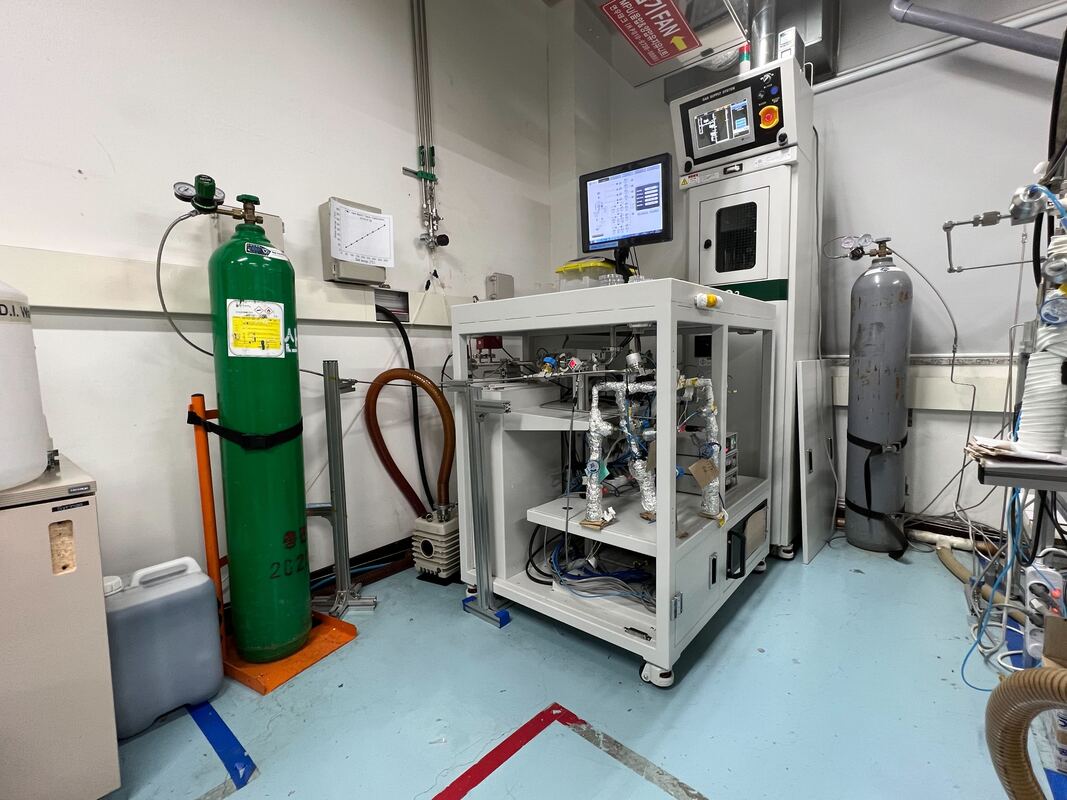
G2 Bldg 8, rm 382 |
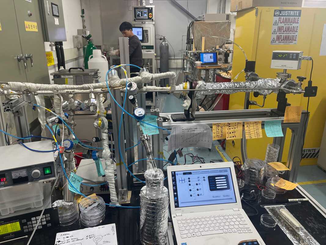
mini ALD Bldg 8, rm 382 |
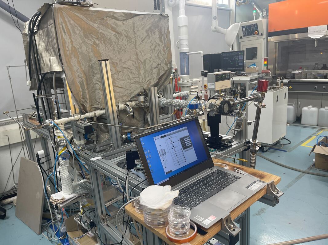
OLD Bldg 8, rm 382 |
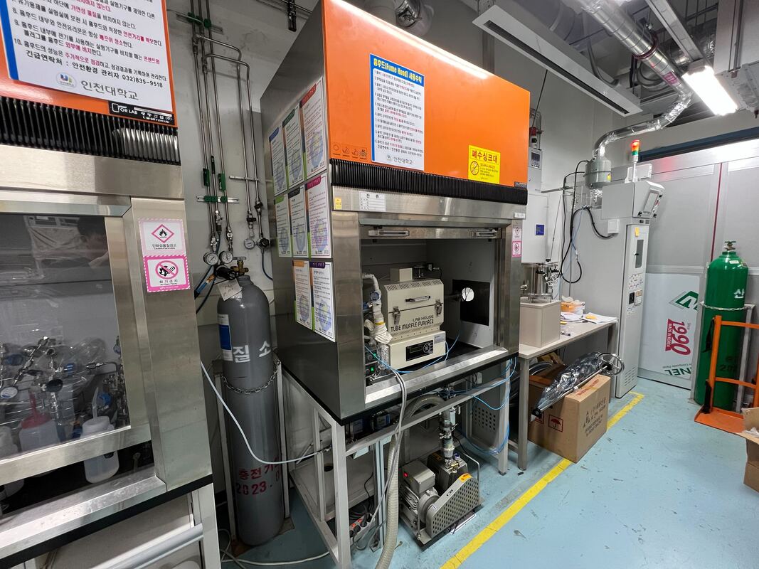
AG Bldg 8, rm 382 |
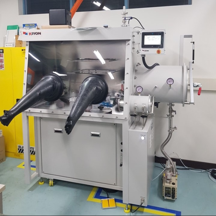
Glove Box Bldg 8, rm 382 |
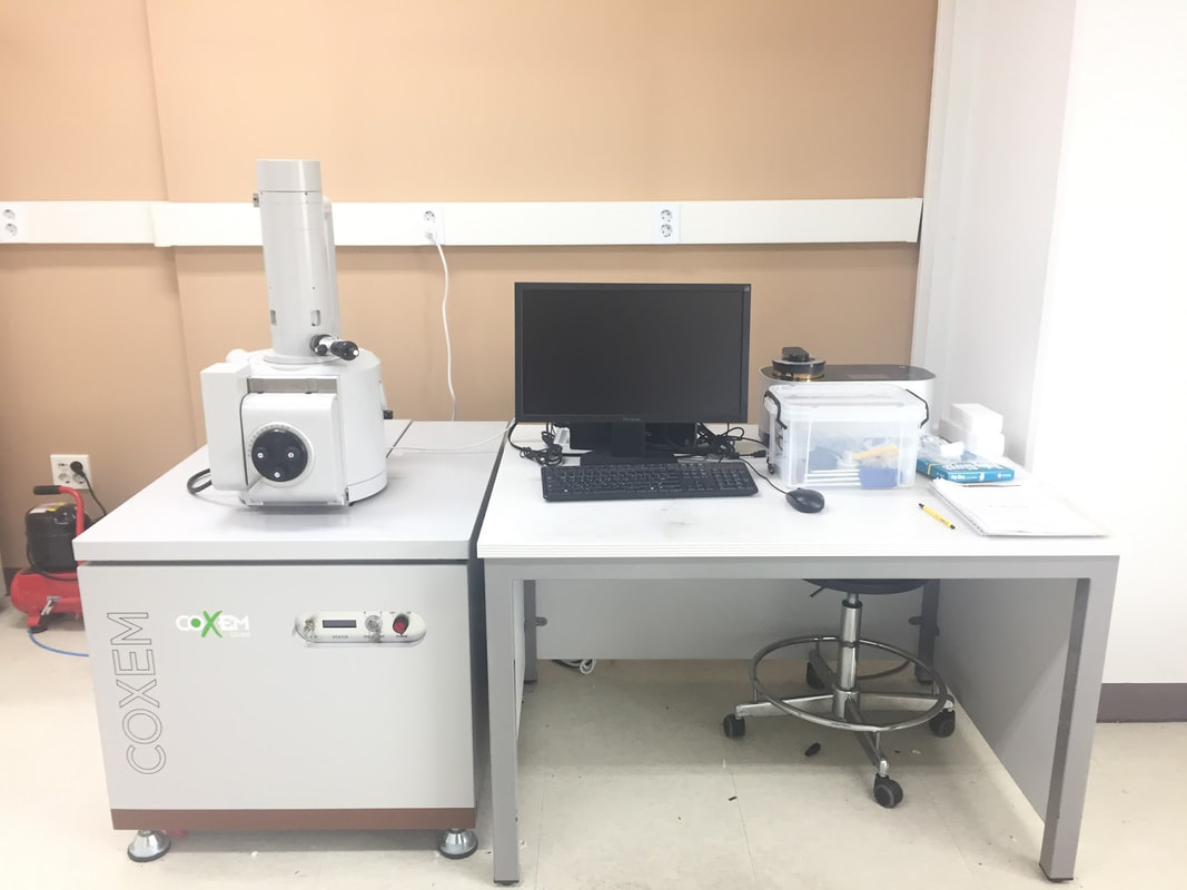
Thermal SEM Bldg 28, rm 312 |
Contact Angle Measurement Bldg 8, rm 382 |
4-point Probe Bldg 8, rm 382 |
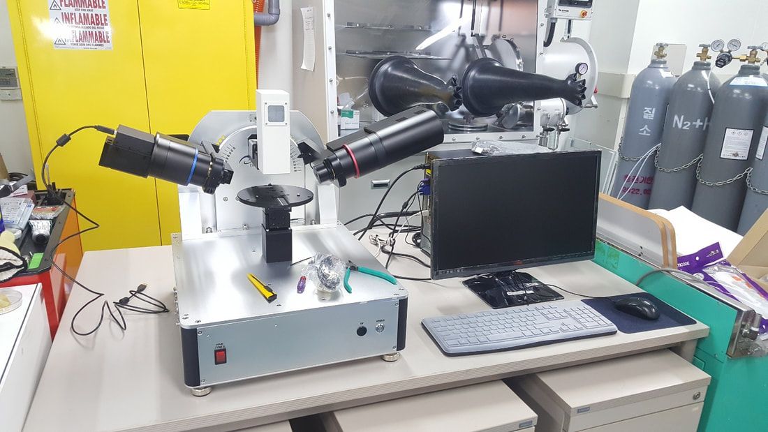
Ellipsometry BLdg 8, RM 382 |
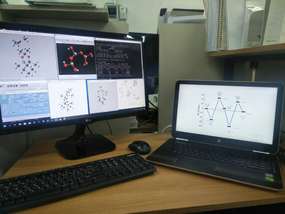
DFT calculation workstation BLDG 8, RM 371 |
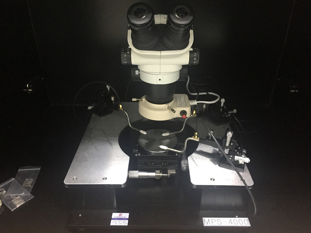
Probe Station Bldg 28, rm 312 |
Spin coater bldg 8, rm 382 |
BET Bldg 28, rm 312 |
Resources
Good reading materials for publication and paper writing
• Writing and organization
1. The Art of the Cover Letter
ACS Nano 2010, 4, 5, 2487-2487, http://dx.doi.org/10.1021/nn100907e
2. The Art of Writing the Title of Your Paper
Chem. Mater. 2014, 26, 11, 3349-3350, http://dx.doi.org/10.1021/cm5017917
3. What’s in a Name?
Chem. Mater. 2014, 26, 11, 3349-3350, http://dx.doi.org/10.1021/jz5014888
4. Why Did You Accept My Paper?
J. Phys. Chem. Lett. 2014, 5, 14, 2443-2443, http://dx.doi.org/10.1021/jz501139d
5. The Experimental Section: The Key to Longevity of Your Research
Chem. Mater. 2014, 26, 5, 1765-1766, http://dx.doi.org/10.1021/cm500632c
6. Your Research Results Look Compelling, but Are They Reliable?
Chem. Mater. 2014, 26, 7, 2211-2213, http://dx.doi.org/10.1021/cm5010449
7. Cite with a Sight
J. Phys. Chem. Lett. 2014, 5, 7, 1241-1242, http://dx.doi.org/10.1021/jz500430j
8. Mastering the Art of Scientific Publication
J. Phys. Chem. Lett. 2014, 5, 20, 3519-3521, http://dx.doi.org/10.1021/jz502010v
9. How to Make Your Next Paper Scientifically Effective
J. Phys. Chem. Lett. 2013, 4, 9, 1578-1581, http://dx.doi.org/10.1021/jz4006916
• Figures and artworks
1. Which Font Looks Best in a Figure?
Chem. Mater. 2016, 28, 3, 689-690, http://dx.doi.org/10.1021/acs.chemmater.6b00306
2. Summarize Your Work in 100 Milliseconds or Less... The Importance of the Table of Contents Image
ACS Nano 2011, 5, 10, 7687-7689, http://dx.doi.org/10.1021/nn203713e
3. Titles and Table of Contents Images: The Candy Store Analogy
Chem. Mater. 2014, 26, 3, 1289-1290, http://dx.doi.org/10.1021/cm500170v
4. Graphical Excellence
J. Phys. Chem. Lett. 2014, 5, 12, 2118-2120, http://dx.doi.org/10.1021/jz500997e
5. Figure Size: Please Be Kind to Your Reader
Chem. Mater. 2017, 29, 19, 8021-8022, http://dx.doi.org/10.1021/acs.chemmater.7b04002
6. Table of Contents Images: Science and Beauty = Clarity
Chem. Mater. 2016, 28, 6, 1589-1590, http://dx.doi.org/10.1021/acs.chemmater.6b00928
7. How We Choose Cover Images
Chem. Mater. 2015, 27, 16, 5451-5452, http://dx.doi.org/10.1021/acs.chemmater.5b03094
8. Absolute, Arbitrary, Relative, or Normalized Scale? How to Get the Scale Right
ACS Energy Lett. 2019, 4, 8, 2005-2006, http://dx.doi.org/10.1021/acsenergylett.9b01571
9. Ten Tips for Capturing Figures with Captions
ACS Energy Lett. 2019, 4, 3, 637-638, http://dx.doi.org/10.1021/acsenergylett.9b00253
• Submission, review, and publication
1. Should I Reveal the History of My Manuscript?
Chem. Mater. 2014, 26, 8, 2487-2487, http://dx.doi.org/10.1021/cm501152b
2. Who Are Corresponding Authors?
ACS Nano 2014, 6, 4, 2861-2861, http://dx.doi.org/10.1021/nn301566x
3. Getting your Submission Right and Avoiding Rejection
J. Phys. Chem. Lett. 2012, 3, 21, 3088-3089, http://dx.doi.org/10.1021/jz3014562
4. Rejecting without Review: The Whys, the Hows
ACS Nano 2010, 4, 9, 4963-4964, http://dx.doi.org/10.1021/nn1022318
5. Ten Reasons Why Peer Review Makes Sense
J. Phys. Chem. Lett. 2015, 6, 13, 2588-2589, http://dx.doi.org/10.1021/acs.jpclett.5b01280
6. Overcoming the Myths of the Review Process and Getting Your Paper Ready for Publication
J. Phys. Chem. Lett. 2014, 5, 5, 896-899, http://dx.doi.org/10.1021/jz500162r
7. In Response
ACS Nano 2012, 6, 5, 3643-3645, http://dx.doi.org/10.1021/nn3019046
8. We Take It Personally
ACS Nano 6, 2012, 12, 10417-10419, http://dx.doi.org/10.1021/nn305696y
9. We Editors Are Authors, Too
ACS Energy Lett. 2019, 4, 1, 249-250, http://dx.doi.org/10.1021/acsenergylett.8b02322
10. What Is the Value of Publishing?
ACS Nano 2018, 12, 7, 6345-6346, http://dx.doi.org/10.1021/acsnano.8b05296
• Impact factor and citations
1. The Impact of the Impact Factor
Chem. Mater. 2014, 26, 13, 3871-3872, http://dx.doi.org/10.1021/cm502204r
2. The Increasing Impact of Multimedia and Social Media in Scientific Publications
J. Phys. Chem. Lett. 2014, 5, 1, 233-234, http://dx.doi.org/10.1021/jz402623m
3. Journal Impact Factor and the Real Impact of Your Paper
J. Phys. Chem. Lett. 2015, 6, 15, 3074-3075, http://dx.doi.org/10.1021/acs.jpclett.5b01527
4. Citation Mania: The Good, the Bad, and the Ugly
ACS Energy Lett. 2019, 4, 2, 471-472, http://dx.doi.org/10.1021/acsenergylett.9b00016
5. Most Cited versus Uncited Papers. What Do They Tell Us?
ACS Energy Lett. 2018, 3, 9, 2134-2135, http://dx.doi.org/10.1021/acsenergylett.8b01443
• Miscellaneous
1. Are You Making the Right Presentation at the Scientific Meeting?
ACS Energy Lett. 2017, 2, 2, 408-409, http://dx.doi.org/10.1021/acsenergylett.7b00004
2. Finding Success through Failures
ACS Energy Lett. 2020, 5, 2, 550-551, http://dx.doi.org/10.1021/acsenergylett.0c00062
|
Department of Materials Science and Engineering, Incheon National University
119 Academy-ro, Yeonsu-gu, Incheon, Korea, 22012 Rm. 305 Bldg.8, Incheon National University +82-32-835-8270, hbrlee[at]inu.ac.kr Copyright by the HBRLRG, All Right Reserved |
|